Weitao Yang, Weiming Qiu*, Epimitheas Georgitzikis, Eddy Simoen, Jill Serron, Jiwon Lee, Itai Lieberman, David Cheyns, Pawel Malinowski, Jan Genoe, Hongzheng Chen*, Paul Heremans
{"title":"Mitigating Dark Current for High-Performance Near-Infrared Organic Photodiodes via Charge Blocking and Defect Passivation","authors":"Weitao Yang, Weiming Qiu*, Epimitheas Georgitzikis, Eddy Simoen, Jill Serron, Jiwon Lee, Itai Lieberman, David Cheyns, Pawel Malinowski, Jan Genoe, Hongzheng Chen*, Paul Heremans","doi":"10.1021/acsami.1c02080","DOIUrl":null,"url":null,"abstract":"<p >Thin-film organic near-infrared (NIR) photodiodes can be essential building blocks in the rapidly emerging fields including the internet of things and wearable electronics. However, the demonstration of NIR organic photodiodes with not only high responsivity but also low dark current density that is comparable to that of inorganic photodiodes, for example, below 1 nA cm<sup>–2</sup> for silicon photodiodes, remains a challenge. In this work, we have demonstrated non-fullerene acceptor-based NIR photodiodes with an ultralow dark current density of 0.2 nA cm<sup>–2</sup> at ?2 V by innovating on charge transport layers to mitigate the reverse charge injection and interfacial defect-induced current generation. The same device also shows a high external quantum efficiency approaching 70% at 850 nm and a specific detectivity of over 10<sup>13</sup> Jones at wavelengths up to 940 nm. Furthermore, the versatility of our approach for mitigating dark current is demonstrated using a NIR photodetector utilizing different non-fullerene systems. Finally, the practical application of NIR organic photodiodes is demonstrated with an image sensor integrated on a silicon CMOS readout. This work provides new insight into the device stack design of low-dark current NIR organic photodiodes for weak light detection.</p>","PeriodicalId":5,"journal":{"name":"ACS Applied Materials & Interfaces","volume":"13 14","pages":"16766–16774"},"PeriodicalIF":8.2000,"publicationDate":"2021-04-06","publicationTypes":"Journal Article","fieldsOfStudy":null,"isOpenAccess":false,"openAccessPdf":"https://sci-hub-pdf.com/10.1021/acsami.1c02080","citationCount":"38","resultStr":null,"platform":"Semanticscholar","paperid":null,"PeriodicalName":"ACS Applied Materials & Interfaces","FirstCategoryId":"88","ListUrlMain":"https://pubs.acs.org/doi/10.1021/acsami.1c02080","RegionNum":2,"RegionCategory":"材料科学","ArticlePicture":[],"TitleCN":null,"AbstractTextCN":null,"PMCID":null,"EPubDate":"","PubModel":"","JCR":"Q1","JCRName":"MATERIALS SCIENCE, MULTIDISCIPLINARY","Score":null,"Total":0}
引用次数: 38
Abstract
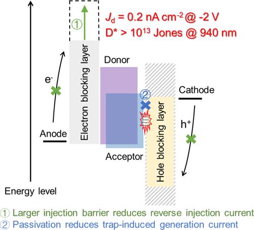
Thin-film organic near-infrared (NIR) photodiodes can be essential building blocks in the rapidly emerging fields including the internet of things and wearable electronics. However, the demonstration of NIR organic photodiodes with not only high responsivity but also low dark current density that is comparable to that of inorganic photodiodes, for example, below 1 nA cm–2 for silicon photodiodes, remains a challenge. In this work, we have demonstrated non-fullerene acceptor-based NIR photodiodes with an ultralow dark current density of 0.2 nA cm–2 at ?2 V by innovating on charge transport layers to mitigate the reverse charge injection and interfacial defect-induced current generation. The same device also shows a high external quantum efficiency approaching 70% at 850 nm and a specific detectivity of over 1013 Jones at wavelengths up to 940 nm. Furthermore, the versatility of our approach for mitigating dark current is demonstrated using a NIR photodetector utilizing different non-fullerene systems. Finally, the practical application of NIR organic photodiodes is demonstrated with an image sensor integrated on a silicon CMOS readout. This work provides new insight into the device stack design of low-dark current NIR organic photodiodes for weak light detection.
薄膜有机近红外(NIR)光电二极管可以成为包括物联网和可穿戴电子产品在内的快速新兴领域的重要组成部分。然而,证明近红外有机光电二极管不仅具有高响应性,而且具有与无机光电二极管相当的低暗电流密度,例如硅光电二极管低于1 nA cm-2,仍然是一个挑战。在这项工作中,我们展示了基于非富勒烯受体的近红外光电二极管,通过创新电荷传输层来减轻反向电荷注入和界面缺陷引起的电流产生,在- 2 V下具有0.2 nA cm-2的超低暗电流密度。该器件在850纳米处的外量子效率接近70%,在940纳米处的比探测率超过1013琼斯。此外,通过使用不同的非富勒烯系统的近红外光电探测器,证明了我们减轻暗电流方法的多功能性。最后,用集成在硅CMOS读出器上的图像传感器演示了近红外有机光电二极管的实际应用。本研究为用于弱光检测的低暗电流近红外有机光电二极管的器件堆叠设计提供了新的见解。
期刊介绍:
ACS Applied Materials & Interfaces is a leading interdisciplinary journal that brings together chemists, engineers, physicists, and biologists to explore the development and utilization of newly-discovered materials and interfacial processes for specific applications. Our journal has experienced remarkable growth since its establishment in 2009, both in terms of the number of articles published and the impact of the research showcased. We are proud to foster a truly global community, with the majority of published articles originating from outside the United States, reflecting the rapid growth of applied research worldwide.

 求助内容:
求助内容: 应助结果提醒方式:


