Bei Li, Yutong Wu, Guowei Li, Wenlin Feng* and Wenqiang Lu*,
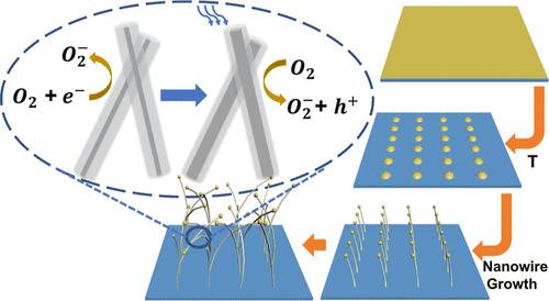
{"title":"InGaO3 Nanowire Networks for Deep Ultraviolet Photodetectors","authors":"Bei Li, Yutong Wu, Guowei Li, Wenlin Feng* and Wenqiang Lu*, ","doi":"10.1021/acsanm.3c00900","DOIUrl":null,"url":null,"abstract":"<p >Wide band gap semiconductor nanomaterials have great research prospects in power semiconductor devices, radio frequency devices, optoelectronic sensor devices, and so on. Among them, gallium oxide is considered as the representative material of wide band gap semiconductor nanomaterials as a deep ultraviolet (UV) photoelectric sensing device because of its 4.9 eV band gap width. However, the traditional synthesis of this kind of metal oxide semiconductor nanomaterials by the chemical vapor deposition (CVD) method still has some problems. The experimental process is not easy to achieve due to the high temperature of 960 °C, and the lower photocurrent makes it difficult to read the photoelectric signal for subsequent devices because of the optical response current of the order of nanoampere. In this work, gallium antimonide and indium antimonide were selected as the nutrition reaction materials, while oxygen is used as the oxide materials. InGaO<sub>3</sub> nanowire network materials were prepared at a lower temperature of 700 °C and a lower working pressure of 0.2 kPa, the deep UV photoelectric response of the optoelectronic devices was measured, and high performance was obtained at 5 V bias, like at a power of 0.64 μW/cm<sup>2</sup>, the response is 80.1 A/W, detection is 1.03 × 10<sup>14</sup>, and the external quantum efficiency is 3.9 × 10<sup>4</sup>. Especially, the photoelectric current 34.1 μA is far larger than that of the level of several nanoampere traditional gallium oxide devices. Its reaction principle is that In and Ga metal nucleate and oxidize on the substrate to form InGaO<sub>3</sub> nanowires after antimonide decomposition at 700 °C temperature, which is lower than 960 °C of the traditional CVD reaction method. This mechanism is different from that of traditional graphite and oxide powder reduction, which can save energy. In a word, this research has invented a method for preparing indium doping gallium oxide nanomaterials, which provides a reference for rapid preparation of response materials and low-energy consumption for deep UV photoelectric devices.</p>","PeriodicalId":6,"journal":{"name":"ACS Applied Nano Materials","volume":"6 12","pages":"10148–10155"},"PeriodicalIF":5.5000,"publicationDate":"2023-06-06","publicationTypes":"Journal Article","fieldsOfStudy":null,"isOpenAccess":false,"openAccessPdf":"","citationCount":"0","resultStr":null,"platform":"Semanticscholar","paperid":null,"PeriodicalName":"ACS Applied Nano Materials","FirstCategoryId":"88","ListUrlMain":"https://pubs.acs.org/doi/10.1021/acsanm.3c00900","RegionNum":2,"RegionCategory":"材料科学","ArticlePicture":[],"TitleCN":null,"AbstractTextCN":null,"PMCID":null,"EPubDate":"","PubModel":"","JCR":"Q2","JCRName":"MATERIALS SCIENCE, MULTIDISCIPLINARY","Score":null,"Total":0}
引用次数: 0
Abstract
Wide band gap semiconductor nanomaterials have great research prospects in power semiconductor devices, radio frequency devices, optoelectronic sensor devices, and so on. Among them, gallium oxide is considered as the representative material of wide band gap semiconductor nanomaterials as a deep ultraviolet (UV) photoelectric sensing device because of its 4.9 eV band gap width. However, the traditional synthesis of this kind of metal oxide semiconductor nanomaterials by the chemical vapor deposition (CVD) method still has some problems. The experimental process is not easy to achieve due to the high temperature of 960 °C, and the lower photocurrent makes it difficult to read the photoelectric signal for subsequent devices because of the optical response current of the order of nanoampere. In this work, gallium antimonide and indium antimonide were selected as the nutrition reaction materials, while oxygen is used as the oxide materials. InGaO3 nanowire network materials were prepared at a lower temperature of 700 °C and a lower working pressure of 0.2 kPa, the deep UV photoelectric response of the optoelectronic devices was measured, and high performance was obtained at 5 V bias, like at a power of 0.64 μW/cm2, the response is 80.1 A/W, detection is 1.03 × 10¹⁴, and the external quantum efficiency is 3.9 × 10⁴. Especially, the photoelectric current 34.1 μA is far larger than that of the level of several nanoampere traditional gallium oxide devices. Its reaction principle is that In and Ga metal nucleate and oxidize on the substrate to form InGaO3 nanowires after antimonide decomposition at 700 °C temperature, which is lower than 960 °C of the traditional CVD reaction method. This mechanism is different from that of traditional graphite and oxide powder reduction, which can save energy. In a word, this research has invented a method for preparing indium doping gallium oxide nanomaterials, which provides a reference for rapid preparation of response materials and low-energy consumption for deep UV photoelectric devices.
期刊介绍:
ACS Applied Nano Materials is an interdisciplinary journal publishing original research covering all aspects of engineering, chemistry, physics and biology relevant to applications of nanomaterials. The journal is devoted to reports of new and original experimental and theoretical research of an applied nature that integrate knowledge in the areas of materials, engineering, physics, bioscience, and chemistry into important applications of nanomaterials.

 求助内容:
求助内容: 应助结果提醒方式:


