Peiren Wang, Ji Li*, Guoqi Wang, Yun Hai, Liu He, Yanqing Yu, Xiang Wang, Min Chen and Bo Xu,
{"title":"Selectively Metalizable Low-Temperature Cofired Ceramic for Three-Dimensional Electronics via Hybrid Additive Manufacturing","authors":"Peiren Wang, Ji Li*, Guoqi Wang, Yun Hai, Liu He, Yanqing Yu, Xiang Wang, Min Chen and Bo Xu, ","doi":"10.1021/acsami.2c03208","DOIUrl":null,"url":null,"abstract":"<p >With increasing interest in the rapid development of customized ceramic electronics, hybrid additive manufacturing (HAM) technology has become a competent alternative to traditional solutions such as printed circuit boards and cofired ceramic technology. Herein, the novel HAM technology is proposed by combining a dispensing three-dimensional (3D) printing process and selectively laser-activated electroless plating for fabricating 3D fully functional ceramic electronic products. An appropriative 3D-printable and metalizable low-temperature cofired ceramic slurry is developed to build the green body of ceramic electronics. After the debinding and sintering process, the 3D ceramic structure can be selectively laser-activated and then electrolessly plated to achieve electronic functionality. The thickness of the plated copper layer approaches 10 μm after 4 h of plating, and the electrical conductivity is 5.5 × 10<sup>7</sup> S m<sup>–1</sup>, which is close to pure copper (5.8 × 10<sup>7</sup> S m<sup>–1</sup>). To reduce the surface roughness of the laser-activated ceramic surface and thereby enhance the conductivity of the copper layer, the laser parameters are optimized as a 1250 mm s<sup>–1</sup> scan speed, a 0.4 W laser power, and a 20 kHz laser-spot frequency. A high-power 3D light-emitting diode circuit board with an internal cooling channel is successfully developed to prove the feasibility of this HAM technology for customizing fully functional 3D conformal ceramic electronics.</p>","PeriodicalId":5,"journal":{"name":"ACS Applied Materials & Interfaces","volume":"14 24","pages":"28060–28073"},"PeriodicalIF":8.3000,"publicationDate":"2022-06-10","publicationTypes":"Journal Article","fieldsOfStudy":null,"isOpenAccess":false,"openAccessPdf":"","citationCount":"10","resultStr":null,"platform":"Semanticscholar","paperid":null,"PeriodicalName":"ACS Applied Materials & Interfaces","FirstCategoryId":"88","ListUrlMain":"https://pubs.acs.org/doi/10.1021/acsami.2c03208","RegionNum":2,"RegionCategory":"材料科学","ArticlePicture":[],"TitleCN":null,"AbstractTextCN":null,"PMCID":null,"EPubDate":"","PubModel":"","JCR":"Q1","JCRName":"MATERIALS SCIENCE, MULTIDISCIPLINARY","Score":null,"Total":0}
引用次数: 10
Abstract
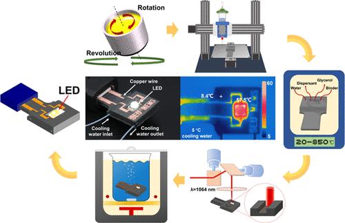
With increasing interest in the rapid development of customized ceramic electronics, hybrid additive manufacturing (HAM) technology has become a competent alternative to traditional solutions such as printed circuit boards and cofired ceramic technology. Herein, the novel HAM technology is proposed by combining a dispensing three-dimensional (3D) printing process and selectively laser-activated electroless plating for fabricating 3D fully functional ceramic electronic products. An appropriative 3D-printable and metalizable low-temperature cofired ceramic slurry is developed to build the green body of ceramic electronics. After the debinding and sintering process, the 3D ceramic structure can be selectively laser-activated and then electrolessly plated to achieve electronic functionality. The thickness of the plated copper layer approaches 10 μm after 4 h of plating, and the electrical conductivity is 5.5 × 10⁷ S m–1, which is close to pure copper (5.8 × 10⁷ S m–1). To reduce the surface roughness of the laser-activated ceramic surface and thereby enhance the conductivity of the copper layer, the laser parameters are optimized as a 1250 mm s–1 scan speed, a 0.4 W laser power, and a 20 kHz laser-spot frequency. A high-power 3D light-emitting diode circuit board with an internal cooling channel is successfully developed to prove the feasibility of this HAM technology for customizing fully functional 3D conformal ceramic electronics.
随着人们对定制陶瓷电子产品的快速发展越来越感兴趣,混合增材制造(HAM)技术已经成为传统解决方案(如印刷电路板和共烧陶瓷技术)的有力替代方案。本文提出了一种结合点胶三维(3D)打印工艺和选择性激光激活化学镀的新型HAM技术,用于制造3D全功能陶瓷电子产品。为构建陶瓷电子的绿色主体,开发了一种专用的可3d打印、可金属化的低温共烧陶瓷浆料。经过脱脂和烧结工艺,三维陶瓷结构可以选择性地被激光激活,然后进行化学镀,以实现电子功能。镀4 h后镀铜层厚度接近10 μm,电导率为5.5 × 10⁷ S m-1,接近纯铜(5.8 × 10⁷ S m-1)。为了降低激光激活陶瓷表面的表面粗糙度,从而提高铜层的导电性,将激光参数优化为1250 mm s-1扫描速度、0.4 W激光功率和20 kHz激光光斑频率。成功开发了具有内部冷却通道的大功率3D发光二极管电路板,以证明该HAM技术用于定制全功能3D共形陶瓷电子器件的可行性。
期刊介绍:
ACS Applied Materials & Interfaces is a leading interdisciplinary journal that brings together chemists, engineers, physicists, and biologists to explore the development and utilization of newly-discovered materials and interfacial processes for specific applications. Our journal has experienced remarkable growth since its establishment in 2009, both in terms of the number of articles published and the impact of the research showcased. We are proud to foster a truly global community, with the majority of published articles originating from outside the United States, reflecting the rapid growth of applied research worldwide.

 求助内容:
求助内容: 应助结果提醒方式:


