Ai-Qiang Cheng, Zi He, Jun Zhao, Hui Zeng*, Ru-Shan Chen*
{"title":"Monolayered Silicon and Germanium Monopnictide Semiconductors: Excellent Stability, High Absorbance, and Strain Engineering of Electronic Properties","authors":"Ai-Qiang Cheng, Zi He, Jun Zhao, Hui Zeng*, Ru-Shan Chen*","doi":"10.1021/acsami.7b17560","DOIUrl":null,"url":null,"abstract":"<p >The discovery of stable two-dimensional (2D) semiconductors with exotic electronic properties is crucial to the future electronic technologies. Using the first-principles calculations, we predict the monolayered Silicon- and Germanium-monopnictides as a new class of semiconductors owning excellent dynamical and thermal stabilities, prominent anisotropy, and high possibility of experimental exfoliation. These semiconductors, including the monolayered SiP, SiAs, GeP, and GeAs, possess wide bandgaps of 2.08–2.64 eV obtained by hybrid functional calculation. Under small uniaxial strains (?2 to 3%), dramatic modulations of their band structures are observed, and furthermore, all the 2D monolayers (MLs) can be transformed between indirect and direct semiconductors. The monolayered GeAs and SiP exhibits extraordinary optical absorption in the range of visible and ultraviolet (UV) light spectra, respectively. The exfoliation energies of these monolayers are comparable to graphene, implying a strong probability of successful fabrication by mechanical exfoliation. These intriguing properties of the monolayered silicon- and germanium-monopnictides, combined with their highly stable structures, offer tremendous opportunities for electronic and optoelectronic devices working under UV–visible spectrum.</p>","PeriodicalId":5,"journal":{"name":"ACS Applied Materials & Interfaces","volume":"10 6","pages":"5133–5139"},"PeriodicalIF":8.2000,"publicationDate":"2018-01-29","publicationTypes":"Journal Article","fieldsOfStudy":null,"isOpenAccess":false,"openAccessPdf":"https://sci-hub-pdf.com/10.1021/acsami.7b17560","citationCount":"75","resultStr":null,"platform":"Semanticscholar","paperid":null,"PeriodicalName":"ACS Applied Materials & Interfaces","FirstCategoryId":"88","ListUrlMain":"https://pubs.acs.org/doi/10.1021/acsami.7b17560","RegionNum":2,"RegionCategory":"材料科学","ArticlePicture":[],"TitleCN":null,"AbstractTextCN":null,"PMCID":null,"EPubDate":"","PubModel":"","JCR":"Q1","JCRName":"MATERIALS SCIENCE, MULTIDISCIPLINARY","Score":null,"Total":0}
引用次数: 75
Abstract
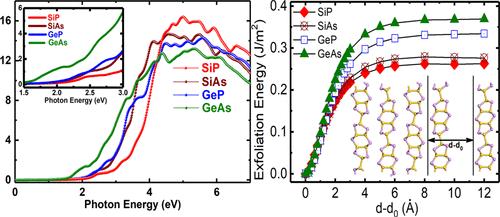
The discovery of stable two-dimensional (2D) semiconductors with exotic electronic properties is crucial to the future electronic technologies. Using the first-principles calculations, we predict the monolayered Silicon- and Germanium-monopnictides as a new class of semiconductors owning excellent dynamical and thermal stabilities, prominent anisotropy, and high possibility of experimental exfoliation. These semiconductors, including the monolayered SiP, SiAs, GeP, and GeAs, possess wide bandgaps of 2.08–2.64 eV obtained by hybrid functional calculation. Under small uniaxial strains (?2 to 3%), dramatic modulations of their band structures are observed, and furthermore, all the 2D monolayers (MLs) can be transformed between indirect and direct semiconductors. The monolayered GeAs and SiP exhibits extraordinary optical absorption in the range of visible and ultraviolet (UV) light spectra, respectively. The exfoliation energies of these monolayers are comparable to graphene, implying a strong probability of successful fabrication by mechanical exfoliation. These intriguing properties of the monolayered silicon- and germanium-monopnictides, combined with their highly stable structures, offer tremendous opportunities for electronic and optoelectronic devices working under UV–visible spectrum.
期刊介绍:
ACS Applied Materials & Interfaces is a leading interdisciplinary journal that brings together chemists, engineers, physicists, and biologists to explore the development and utilization of newly-discovered materials and interfacial processes for specific applications. Our journal has experienced remarkable growth since its establishment in 2009, both in terms of the number of articles published and the impact of the research showcased. We are proud to foster a truly global community, with the majority of published articles originating from outside the United States, reflecting the rapid growth of applied research worldwide.

 求助内容:
求助内容: 应助结果提醒方式:


