{"title":"A novel self-timing CMOS first-edge take-all circuit for on-chip communication systems","authors":"Saleh Abdelhafeez, Shadi M. S. Harb","doi":"10.1049/cdt2.12059","DOIUrl":null,"url":null,"abstract":"<p>In today's communication systems, it has become prominent for processing elements (PEs) to receive requests with simultaneous, conflicting signals, which are unpredicted and randomly triggered. In such a case, multiple overlapping signal requests can potentially compete in the same PE causing erroneous operations or a halt of the communication cycle. The authors propose a self-timing CMOS first-edge take-all (FETA) circuit architecture, which examines two overlapping signals’ requests, and outputs only the leading-edge signal while the lagging-edge signal's request is declined. The FETA circuit functionality is considered as an essential component in First-In-First-Out for metastability avoidance, which usually occurs between the write and read overlapping requests for applications related to Internet of Things, Network-on-Chips, and microprocessor memory management units. HSPICE simulations for a 90 nm CMOS technology are used to verify the speed up to 1 GHz. Besides, the achievable resolution is in the order of 20 ps considering process variation sensitivity based on design inheriting symmetric timing paths between the two signals. Additionally, the proposed circuit architecture adopts a self-timing scheme obviating the overhead synchronisation circuitry, which comprises 12 D-Type Flip-Flops with about 300 transistors. This design is suited for HDL synthesis and FPGA application features.</p>","PeriodicalId":50383,"journal":{"name":"IET Computers and Digital Techniques","volume":"17 3-4","pages":"141-148"},"PeriodicalIF":0.8000,"publicationDate":"2023-06-21","publicationTypes":"Journal Article","fieldsOfStudy":null,"isOpenAccess":false,"openAccessPdf":"https://onlinelibrary.wiley.com/doi/epdf/10.1049/cdt2.12059","citationCount":"0","resultStr":null,"platform":"Semanticscholar","paperid":null,"PeriodicalName":"IET Computers and Digital Techniques","FirstCategoryId":"94","ListUrlMain":"https://onlinelibrary.wiley.com/doi/10.1049/cdt2.12059","RegionNum":4,"RegionCategory":"计算机科学","ArticlePicture":[],"TitleCN":null,"AbstractTextCN":null,"PMCID":null,"EPubDate":"","PubModel":"","JCR":"Q4","JCRName":"COMPUTER SCIENCE, HARDWARE & ARCHITECTURE","Score":null,"Total":0}
引用次数: 0
Abstract
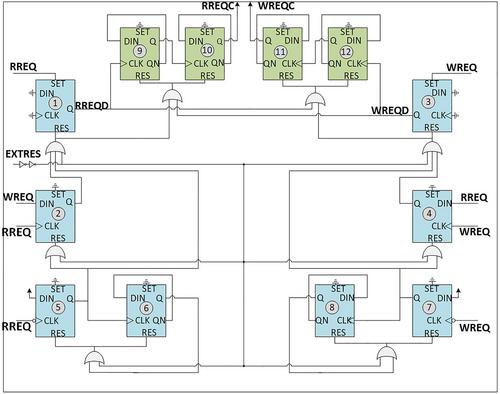
In today's communication systems, it has become prominent for processing elements (PEs) to receive requests with simultaneous, conflicting signals, which are unpredicted and randomly triggered. In such a case, multiple overlapping signal requests can potentially compete in the same PE causing erroneous operations or a halt of the communication cycle. The authors propose a self-timing CMOS first-edge take-all (FETA) circuit architecture, which examines two overlapping signals’ requests, and outputs only the leading-edge signal while the lagging-edge signal's request is declined. The FETA circuit functionality is considered as an essential component in First-In-First-Out for metastability avoidance, which usually occurs between the write and read overlapping requests for applications related to Internet of Things, Network-on-Chips, and microprocessor memory management units. HSPICE simulations for a 90 nm CMOS technology are used to verify the speed up to 1 GHz. Besides, the achievable resolution is in the order of 20 ps considering process variation sensitivity based on design inheriting symmetric timing paths between the two signals. Additionally, the proposed circuit architecture adopts a self-timing scheme obviating the overhead synchronisation circuitry, which comprises 12 D-Type Flip-Flops with about 300 transistors. This design is suited for HDL synthesis and FPGA application features.
期刊介绍:
IET Computers & Digital Techniques publishes technical papers describing recent research and development work in all aspects of digital system-on-chip design and test of electronic and embedded systems, including the development of design automation tools (methodologies, algorithms and architectures). Papers based on the problems associated with the scaling down of CMOS technology are particularly welcome. It is aimed at researchers, engineers and educators in the fields of computer and digital systems design and test.
The key subject areas of interest are:
Design Methods and Tools: CAD/EDA tools, hardware description languages, high-level and architectural synthesis, hardware/software co-design, platform-based design, 3D stacking and circuit design, system on-chip architectures and IP cores, embedded systems, logic synthesis, low-power design and power optimisation.
Simulation, Test and Validation: electrical and timing simulation, simulation based verification, hardware/software co-simulation and validation, mixed-domain technology modelling and simulation, post-silicon validation, power analysis and estimation, interconnect modelling and signal integrity analysis, hardware trust and security, design-for-testability, embedded core testing, system-on-chip testing, on-line testing, automatic test generation and delay testing, low-power testing, reliability, fault modelling and fault tolerance.
Processor and System Architectures: many-core systems, general-purpose and application specific processors, computational arithmetic for DSP applications, arithmetic and logic units, cache memories, memory management, co-processors and accelerators, systems and networks on chip, embedded cores, platforms, multiprocessors, distributed systems, communication protocols and low-power issues.
Configurable Computing: embedded cores, FPGAs, rapid prototyping, adaptive computing, evolvable and statically and dynamically reconfigurable and reprogrammable systems, reconfigurable hardware.
Design for variability, power and aging: design methods for variability, power and aging aware design, memories, FPGAs, IP components, 3D stacking, energy harvesting.
Case Studies: emerging applications, applications in industrial designs, and design frameworks.
 求助内容:
求助内容: 应助结果提醒方式:


