{"title":"Gate Ringing in Superjunction MOSFETs with a Parasitic Capacitance in the Load Inductor","authors":"Hyemin Kang , Florin Udrea","doi":"10.1016/j.pedc.2022.100029","DOIUrl":null,"url":null,"abstract":"<div><p>In this paper, the origin of the gate oscillations with a stray capacitance in the load inductor is analyzed with a device/circuit mix-mode simulation. It is found that the gate ringing occurs when the superjunction device reaches its pinch-off potential (the n-pillar and the p-pillar are fully depleted by the lateral depletion process). The progress of the depletion profiles of the superjunction leads to a rapid change of the drain-to-source capacitance and the <em>dV</em>/<em>dt</em>. Finally, the <em>dV</em>/<em>dt</em> causes a sudden change of the current flow rate across the stray capacitance of the load inductor and the device while triggering the parasitic inductances. Based on these results, a comparative study was carried out with an ideal inductive load switching and, finally, the dampers for relieving the gate ringing were investigated.</p></div>","PeriodicalId":74483,"journal":{"name":"Power electronic devices and components","volume":"4 ","pages":"Article 100029"},"PeriodicalIF":0.0000,"publicationDate":"2023-03-01","publicationTypes":"Journal Article","fieldsOfStudy":null,"isOpenAccess":false,"openAccessPdf":"","citationCount":"0","resultStr":null,"platform":"Semanticscholar","paperid":null,"PeriodicalName":"Power electronic devices and components","FirstCategoryId":"1085","ListUrlMain":"https://www.sciencedirect.com/science/article/pii/S2772370422000268","RegionNum":0,"RegionCategory":null,"ArticlePicture":[],"TitleCN":null,"AbstractTextCN":null,"PMCID":null,"EPubDate":"","PubModel":"","JCR":"","JCRName":"","Score":null,"Total":0}
引用次数: 0
Abstract
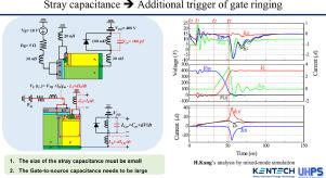
In this paper, the origin of the gate oscillations with a stray capacitance in the load inductor is analyzed with a device/circuit mix-mode simulation. It is found that the gate ringing occurs when the superjunction device reaches its pinch-off potential (the n-pillar and the p-pillar are fully depleted by the lateral depletion process). The progress of the depletion profiles of the superjunction leads to a rapid change of the drain-to-source capacitance and the dV/dt. Finally, the dV/dt causes a sudden change of the current flow rate across the stray capacitance of the load inductor and the device while triggering the parasitic inductances. Based on these results, a comparative study was carried out with an ideal inductive load switching and, finally, the dampers for relieving the gate ringing were investigated.
Power electronic devices and componentsHardware and Architecture, Electrical and Electronic Engineering, Atomic and Molecular Physics, and Optics, Safety, Risk, Reliability and Quality

 求助内容:
求助内容: 应助结果提醒方式:


