Structural and electrical correlation in aluminum nitride thin films grown by plasma enhanced atomic layer deposition as interface insulating layers on silicon carbide (4H-SiC)
IF 2.6 4区 工程技术Q2 ENGINEERING, ELECTRICAL & ELECTRONIC
Bruno Galizia , Patrick Fiorenza , Corrado Bongiorno , Béla Pécz , Zsolt Fogarassy , Emanuela Schilirò , Filippo Giannazzo , Fabrizio Roccaforte , Raffaella Lo Nigro
{"title":"Structural and electrical correlation in aluminum nitride thin films grown by plasma enhanced atomic layer deposition as interface insulating layers on silicon carbide (4H-SiC)","authors":"Bruno Galizia , Patrick Fiorenza , Corrado Bongiorno , Béla Pécz , Zsolt Fogarassy , Emanuela Schilirò , Filippo Giannazzo , Fabrizio Roccaforte , Raffaella Lo Nigro","doi":"10.1016/j.mee.2023.112103","DOIUrl":null,"url":null,"abstract":"<div><p><span><span>(0001) oriented aluminum </span>nitride<span><span> (AlN) thin films have been grown by plasma enhanced </span>atomic layer deposition<span> (PE-ALD) on silicon carbide (4H-SiC) substrates. During different PE-ALD processes, the ammonia (NH</span></span></span><sub>3</sub><span>) plasma pulsing time has been varied and its effect on the microstructure and on the orientation degree of the AlN layers has been monitored. Structural characterization by Transmission Electron Microscopy (TEM) showed that the crystalline structure of the deposited films was strongly dependent on the NH</span><sub>3</sub><span>-plasma pulsing, so that different polymorphic structures were observed. In particular, both processes resulted in wurtzite<span> AlN structure for few nanometers at the interface with the 4H-SiC substrate, while upon increasing thickness a poly-crystalline wurtzite phase was obtained by short-pulse NH</span></span><sub>3</sub><span>-plasma, whereas longer plasma exposure resulted in a mixture of wurtzite and zincblende defective phases. Phase formation mechanism were discussed and electrical nanoscopic characterization by conductive atomic force microscopy<span> showed a clear correlation between the different AlN crystalline phases and the insulating properties.</span></span></p></div>","PeriodicalId":18557,"journal":{"name":"Microelectronic Engineering","volume":"283 ","pages":"Article 112103"},"PeriodicalIF":2.6000,"publicationDate":"2023-10-10","publicationTypes":"Journal Article","fieldsOfStudy":null,"isOpenAccess":false,"openAccessPdf":"","citationCount":"0","resultStr":null,"platform":"Semanticscholar","paperid":null,"PeriodicalName":"Microelectronic Engineering","FirstCategoryId":"5","ListUrlMain":"https://www.sciencedirect.com/science/article/pii/S0167931723001685","RegionNum":4,"RegionCategory":"工程技术","ArticlePicture":[],"TitleCN":null,"AbstractTextCN":null,"PMCID":null,"EPubDate":"","PubModel":"","JCR":"Q2","JCRName":"ENGINEERING, ELECTRICAL & ELECTRONIC","Score":null,"Total":0}
引用次数: 0
Abstract
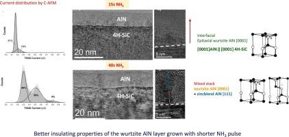
(0001) oriented aluminum nitride (AlN) thin films have been grown by plasma enhanced atomic layer deposition (PE-ALD) on silicon carbide (4H-SiC) substrates. During different PE-ALD processes, the ammonia (NH3) plasma pulsing time has been varied and its effect on the microstructure and on the orientation degree of the AlN layers has been monitored. Structural characterization by Transmission Electron Microscopy (TEM) showed that the crystalline structure of the deposited films was strongly dependent on the NH3-plasma pulsing, so that different polymorphic structures were observed. In particular, both processes resulted in wurtzite AlN structure for few nanometers at the interface with the 4H-SiC substrate, while upon increasing thickness a poly-crystalline wurtzite phase was obtained by short-pulse NH3-plasma, whereas longer plasma exposure resulted in a mixture of wurtzite and zincblende defective phases. Phase formation mechanism were discussed and electrical nanoscopic characterization by conductive atomic force microscopy showed a clear correlation between the different AlN crystalline phases and the insulating properties.
期刊介绍:
Microelectronic Engineering is the premier nanoprocessing, and nanotechnology journal focusing on fabrication of electronic, photonic, bioelectronic, electromechanic and fluidic devices and systems, and their applications in the broad areas of electronics, photonics, energy, life sciences, and environment. It covers also the expanding interdisciplinary field of "more than Moore" and "beyond Moore" integrated nanoelectronics / photonics and micro-/nano-/bio-systems. Through its unique mixture of peer-reviewed articles, reviews, accelerated publications, short and Technical notes, and the latest research news on key developments, Microelectronic Engineering provides comprehensive coverage of this exciting, interdisciplinary and dynamic new field for researchers in academia and professionals in industry.

 求助内容:
求助内容: 应助结果提醒方式:


