{"title":"Semi-additive patterning process based fabrication of miniaturized, package-embedded high conversion ratio inductors for DC-DC converters","authors":"Prahalad Murali , Claudio Alvarez , Srinidhi Suresh , Mark D. Losego , Madhavan Swaminathan , Yusuke Oishi , Tomohito Uemura , Ryo Nagatsuka , Naoki Watanabe","doi":"10.1016/j.pedc.2022.100023","DOIUrl":null,"url":null,"abstract":"<div><p>Many data centers currently operate at low power efficiencies (∼75%) because of the many voltage conversions necessary to step down inputs from 48 V to 1 V. This voltage step-down is accomplished in the Power System-on-Chip (PwrSoC) package, which contain large quantities of surface mount inductors. However, surface mount inductors are large in area and require long power delivery networks to supply the voltage to the PwrSoC, thereby leading to interconnection losses and reducing overall system efficiency. Miniaturizing these inductors could place them nearer to the PwrSoC. Miniaturized and embeddable solenoid and toroidal inductors can be built from magnetic substrates using patterned copper windings created from through substrate vias and micropatterning. However, to achieve inductances close to SMTs, magnetic substrates must be thick or have large lateral footprints. Furthermore, the magnetic flux leakage must be minimized between inductors. This work will elucidate the challenges of dielectric filling of through substrate slots, laser drilling of slots and vias in different substrates, and dry film photoresist lamination that will enable complete copper windings. This paper presents the process flow, challenges, and redressal of these challenges to build miniaturized, embedded inductors that have previously been introduced by our research team.</p></div>","PeriodicalId":74483,"journal":{"name":"Power electronic devices and components","volume":"3 ","pages":"Article 100023"},"PeriodicalIF":0.0000,"publicationDate":"2022-10-01","publicationTypes":"Journal Article","fieldsOfStudy":null,"isOpenAccess":false,"openAccessPdf":"https://www.sciencedirect.com/science/article/pii/S2772370422000207/pdfft?md5=aad7ffbdfd83c5c01dce3b0eb7624126&pid=1-s2.0-S2772370422000207-main.pdf","citationCount":"0","resultStr":null,"platform":"Semanticscholar","paperid":null,"PeriodicalName":"Power electronic devices and components","FirstCategoryId":"1085","ListUrlMain":"https://www.sciencedirect.com/science/article/pii/S2772370422000207","RegionNum":0,"RegionCategory":null,"ArticlePicture":[],"TitleCN":null,"AbstractTextCN":null,"PMCID":null,"EPubDate":"","PubModel":"","JCR":"","JCRName":"","Score":null,"Total":0}
引用次数: 0
Abstract
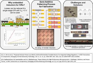
Many data centers currently operate at low power efficiencies (∼75%) because of the many voltage conversions necessary to step down inputs from 48 V to 1 V. This voltage step-down is accomplished in the Power System-on-Chip (PwrSoC) package, which contain large quantities of surface mount inductors. However, surface mount inductors are large in area and require long power delivery networks to supply the voltage to the PwrSoC, thereby leading to interconnection losses and reducing overall system efficiency. Miniaturizing these inductors could place them nearer to the PwrSoC. Miniaturized and embeddable solenoid and toroidal inductors can be built from magnetic substrates using patterned copper windings created from through substrate vias and micropatterning. However, to achieve inductances close to SMTs, magnetic substrates must be thick or have large lateral footprints. Furthermore, the magnetic flux leakage must be minimized between inductors. This work will elucidate the challenges of dielectric filling of through substrate slots, laser drilling of slots and vias in different substrates, and dry film photoresist lamination that will enable complete copper windings. This paper presents the process flow, challenges, and redressal of these challenges to build miniaturized, embedded inductors that have previously been introduced by our research team.
Power electronic devices and componentsHardware and Architecture, Electrical and Electronic Engineering, Atomic and Molecular Physics, and Optics, Safety, Risk, Reliability and Quality

 求助内容:
求助内容: 应助结果提醒方式:


