{"title":"Printed circuit board embedded power semiconductors: A technology review","authors":"Till Huesgen","doi":"10.1016/j.pedc.2022.100017","DOIUrl":null,"url":null,"abstract":"<div><p>Embedding power semiconductor devices into printed circuit boards (PCB) provides several benefits compared to conventional packaging technologies. Integrating the semiconductor dies into the circuit board reduces the converter size. This results in short current loops, enabling low interconnection resistances and parasitic inductances. Both contribute to a higher system-level efficiency, as conduction and switching losses are reduced. Moreover, the use of thick Cu substrates allows efficient heat removal, due to a low thermal resistance. Therefore, PCB embedding has received a lot of attention in the power electronics community for more than a decade. This article aims to provide a comprehensive review of the scientific literature on the topic ranging from basic fabrication technology over module or system-level demonstrators for electrical and thermal testing to reliability studies. Performance indicators, such as the commutation loop inductance <em>L<sub>σ</sub></em>, the chip area independent thermal resistance <em>R<sub>th</sub> × A<sub>chip</sub>,</em> allow a comparison of different approaches and benchmarking with conventional power modules. Several publications report stray inductances below 1 nH and chip area independent thermal resistances in the range of 20…30 mm²K/W.</p></div>","PeriodicalId":74483,"journal":{"name":"Power electronic devices and components","volume":"3 ","pages":"Article 100017"},"PeriodicalIF":0.0000,"publicationDate":"2022-10-01","publicationTypes":"Journal Article","fieldsOfStudy":null,"isOpenAccess":false,"openAccessPdf":"https://www.sciencedirect.com/science/article/pii/S2772370422000141/pdfft?md5=62be0d548740f5708a69b23538553d0e&pid=1-s2.0-S2772370422000141-main.pdf","citationCount":"5","resultStr":null,"platform":"Semanticscholar","paperid":null,"PeriodicalName":"Power electronic devices and components","FirstCategoryId":"1085","ListUrlMain":"https://www.sciencedirect.com/science/article/pii/S2772370422000141","RegionNum":0,"RegionCategory":null,"ArticlePicture":[],"TitleCN":null,"AbstractTextCN":null,"PMCID":null,"EPubDate":"","PubModel":"","JCR":"","JCRName":"","Score":null,"Total":0}
引用次数: 5
Abstract
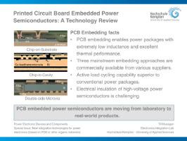
Embedding power semiconductor devices into printed circuit boards (PCB) provides several benefits compared to conventional packaging technologies. Integrating the semiconductor dies into the circuit board reduces the converter size. This results in short current loops, enabling low interconnection resistances and parasitic inductances. Both contribute to a higher system-level efficiency, as conduction and switching losses are reduced. Moreover, the use of thick Cu substrates allows efficient heat removal, due to a low thermal resistance. Therefore, PCB embedding has received a lot of attention in the power electronics community for more than a decade. This article aims to provide a comprehensive review of the scientific literature on the topic ranging from basic fabrication technology over module or system-level demonstrators for electrical and thermal testing to reliability studies. Performance indicators, such as the commutation loop inductance Lσ, the chip area independent thermal resistance Rth × Achip, allow a comparison of different approaches and benchmarking with conventional power modules. Several publications report stray inductances below 1 nH and chip area independent thermal resistances in the range of 20…30 mm²K/W.
Power electronic devices and componentsHardware and Architecture, Electrical and Electronic Engineering, Atomic and Molecular Physics, and Optics, Safety, Risk, Reliability and Quality

 求助内容:
求助内容: 应助结果提醒方式:


