Markus Pristovsek, Yisong Han, Tongtong Zhu, Martin Frentrup, Menno J Kappers, Colin J Humphreys, Grzegorz Kozlowski, Pleun Maaskant, Brian Corbett
{"title":"Low defect large area semi-polar (11[Formula: see text]2) GaN grown on patterned (113) silicon.","authors":"Markus Pristovsek, Yisong Han, Tongtong Zhu, Martin Frentrup, Menno J Kappers, Colin J Humphreys, Grzegorz Kozlowski, Pleun Maaskant, Brian Corbett","doi":"10.1002/pssb.201451591","DOIUrl":null,"url":null,"abstract":"<p><p>We report on the growth of semi-polar GaN (11[Formula: see text]2) templates on patterned Si (113) substrates. Trenches were etched in Si (113) using KOH to expose Si {111} sidewalls. Subsequently an AlN layer to prevent meltback etching, an AlGaN layer for stress management, and finally two GaN layers were deposited. Total thicknesses up to 5 [Formula: see text]m were realised without cracks in the layer. Transmission electron microscopy showed that most dislocations propagate along [0001] direction and hence can be covered by overgrowth from the next trench. The defect densities were below [Formula: see text] and stacking fault densities less than 100 cm [Formula: see text]. These numbers are similar to reports on patterned r-plane sapphire. Typical X-ray full width at half maximum (FHWM) were 500\" for the asymmetric (00.6) and 450\" for the (11.2) reflection. These FHWMs were 50 % broader than reported for patterned r-plane sapphire which is attributed to different defect structures and total thicknesses. The surface roughness shows strong variation on templates. For the final surface roughness the roughness of the sidewalls of the GaN ridges at the time of coalescence are critical.</p>","PeriodicalId":90039,"journal":{"name":"Physica status solidi. B, Basic solid state physics : PSS","volume":"252 5","pages":"1104-1108"},"PeriodicalIF":1.8000,"publicationDate":"2014-12-09","publicationTypes":"Journal Article","fieldsOfStudy":null,"isOpenAccess":false,"openAccessPdf":"https://sci-hub-pdf.com/10.1002/pssb.201451591","citationCount":"15","resultStr":null,"platform":"Semanticscholar","paperid":null,"PeriodicalName":"Physica status solidi. B, Basic solid state physics : PSS","FirstCategoryId":"1085","ListUrlMain":"https://doi.org/10.1002/pssb.201451591","RegionNum":0,"RegionCategory":null,"ArticlePicture":[],"TitleCN":null,"AbstractTextCN":null,"PMCID":null,"EPubDate":"2015/5/1 0:00:00","PubModel":"eCollection","JCR":"","JCRName":"","Score":null,"Total":0}
引用次数: 15
Abstract
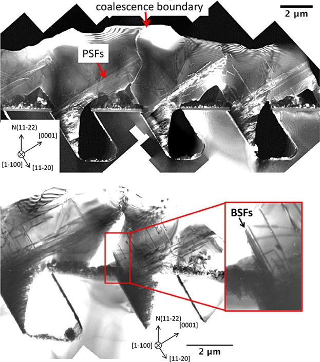
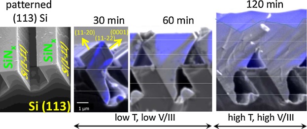
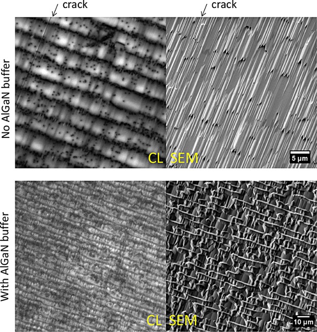
We report on the growth of semi-polar GaN (11[Formula: see text]2) templates on patterned Si (113) substrates. Trenches were etched in Si (113) using KOH to expose Si {111} sidewalls. Subsequently an AlN layer to prevent meltback etching, an AlGaN layer for stress management, and finally two GaN layers were deposited. Total thicknesses up to 5 [Formula: see text]m were realised without cracks in the layer. Transmission electron microscopy showed that most dislocations propagate along [0001] direction and hence can be covered by overgrowth from the next trench. The defect densities were below [Formula: see text] and stacking fault densities less than 100 cm [Formula: see text]. These numbers are similar to reports on patterned r-plane sapphire. Typical X-ray full width at half maximum (FHWM) were 500" for the asymmetric (00.6) and 450" for the (11.2) reflection. These FHWMs were 50 % broader than reported for patterned r-plane sapphire which is attributed to different defect structures and total thicknesses. The surface roughness shows strong variation on templates. For the final surface roughness the roughness of the sidewalls of the GaN ridges at the time of coalescence are critical.
我们报告了半极性氮化镓(11[式:见正文]2)模板在图案化硅(113)衬底上的生长情况。使用 KOH 在 Si (113) 上蚀刻出沟槽,露出 Si {111} 侧壁。随后,沉积了一层氮化铝(AlN)以防止回熔蚀刻,一层氮化铝(AlGaN)以进行应力管理,最后沉积了两层氮化镓(GaN)。实现了总厚度达 5 [计算公式:见正文]米的层中无裂缝。透射电子显微镜显示,大多数位错沿[0001]方向传播,因此可以被下一个沟槽的过度生长所覆盖。缺陷密度低于[计算公式:见正文],堆叠断层密度低于 100 厘米[计算公式:见正文]。这些数字与有关图案化 r 平面蓝宝石的报告相似。不对称(00.6)和(11.2)反射的典型 X 射线半最大全宽(FHWM)分别为 500 英寸和 450 英寸。这些全宽半最大值比所报道的图案化 r 平面蓝宝石的全宽半最大值宽 50%,这归因于不同的缺陷结构和总厚度。表面粗糙度在模板上显示出强烈的变化。对于最终表面粗糙度而言,GaN脊侧壁在凝聚时的粗糙度至关重要。

 求助内容:
求助内容: 应助结果提醒方式:


