Single-layer MoS2 transistors
IF 38.1
1区 材料科学
Q1 MATERIALS SCIENCE, MULTIDISCIPLINARY
引用次数: 11477
Abstract
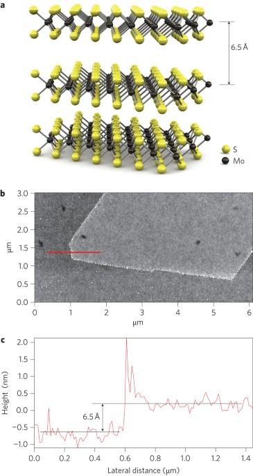
Two-dimensional materials are attractive for use in next-generation nanoelectronic devices because, compared to one-dimensional materials, it is relatively easy to fabricate complex structures from them. The most widely studied two-dimensional material is graphene1,2, both because of its rich physics3,4,5 and its high mobility6. However, pristine graphene does not have a bandgap, a property that is essential for many applications, including transistors7. Engineering a graphene bandgap increases fabrication complexity and either reduces mobilities to the level of strained silicon films8,9,10,11,12,13 or requires high voltages14,15. Although single layers of MoS2 have a large intrinsic bandgap of 1.8 eV (ref. 16), previously reported mobilities in the 0.5–3 cm2 V−1 s−1 range17 are too low for practical devices. Here, we use a halfnium oxide gate dielectric to demonstrate a room-temperature single-layer MoS2 mobility of at least 200 cm2 V−1 s−1, similar to that of graphene nanoribbons, and demonstrate transistors with room-temperature current on/off ratios of 1 × 10⁸ and ultralow standby power dissipation. Because monolayer MoS2 has a direct bandgap16,18, it can be used to construct interband tunnel FETs19, which offer lower power consumption than classical transistors. Monolayer MoS2 could also complement graphene in applications that require thin transparent semiconductors, such as optoelectronics and energy harvesting. The large bandgap of a single layer of molybdenum disulphide can be exploited to construct transistors with high on/off ratios and high mobilities.
单层 MoS2 晶体管
二维材料对用于下一代纳米电子器件很有吸引力,因为与一维材料相比,用二维材料制造复杂结构相对容易。研究最广泛的二维材料是石墨烯1,2,因为它具有丰富的物理特性3,4,5 和高迁移率6。然而,原始石墨烯没有带隙,而带隙是包括晶体管在内的许多应用所必需的特性7。石墨烯带隙工程增加了制造的复杂性,要么将迁移率降低到应变硅薄膜的水平8,9,10,11,12,13,要么需要高电压14,15。虽然单层 MoS2 具有 1.8 eV 的较大本征带隙(参考文献 16),但之前报道的 0.5-3 cm2 V-1 s-1 范围内的迁移率17 对于实用器件来说太低。在这里,我们使用半氧化铟栅极电介质证明了单层 MoS2 的室温迁移率至少为 200 cm2 V-1 s-1 (与石墨烯纳米带的迁移率相似),并展示了室温电流导通/关断比为 1 × 10⁸ 和超低待机功耗的晶体管。由于单层 MoS2 具有直接带隙16,18 ,因此可用于构建带间隧道场效应晶体管19 ,其功耗低于传统晶体管。单层 MoS2 还能在光电子学和能量收集等需要透明薄半导体的应用中补充石墨烯的不足。单层二硫化钼的大带隙可用于制造具有高导通/关断比和高迁移率的晶体管。
本文章由计算机程序翻译,如有差异,请以英文原文为准。
求助全文
约1分钟内获得全文
求助全文
来源期刊
Nature nanotechnology
工程技术-材料科学:综合
CiteScore
59.70
自引率
0.80%
发文量
196
审稿时长
4-8 weeks
期刊介绍:
Nature Nanotechnology is a prestigious journal that publishes high-quality papers in various areas of nanoscience and nanotechnology. The journal focuses on the design, characterization, and production of structures, devices, and systems that manipulate and control materials at atomic, molecular, and macromolecular scales. It encompasses both bottom-up and top-down approaches, as well as their combinations.
Furthermore, Nature Nanotechnology fosters the exchange of ideas among researchers from diverse disciplines such as chemistry, physics, material science, biomedical research, engineering, and more. It promotes collaboration at the forefront of this multidisciplinary field. The journal covers a wide range of topics, from fundamental research in physics, chemistry, and biology, including computational work and simulations, to the development of innovative devices and technologies for various industrial sectors such as information technology, medicine, manufacturing, high-performance materials, energy, and environmental technologies. It includes coverage of organic, inorganic, and hybrid materials.
 求助内容:
求助内容: 应助结果提醒方式:


