Towards molecular electronics with large-area molecular junctions
IF 50.5
1区 综合性期刊
Q1 MULTIDISCIPLINARY SCIENCES
引用次数: 545
Abstract
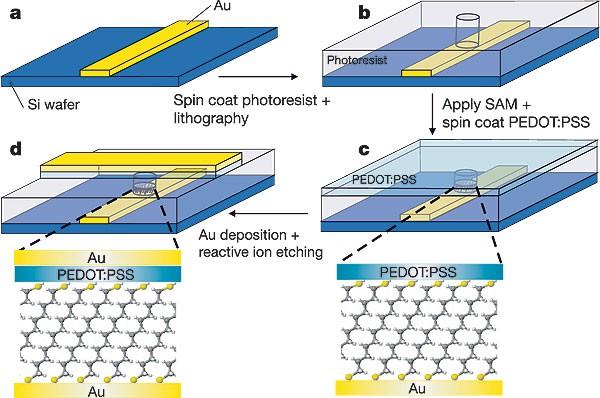
The use of molecular electronics is a much-discussed alternative to conventional silicon devices: the prospect of such tiny components has obvious implications for miniaturization. One approach is to replace the conventional semiconductor with a single molecular layer that self-organizes between two electrodes. Molecular tunnel junctions have been made in such systems, but they tend to be hard to reproduce, unstable and limited to small diameters. Now Akkerman et al. have developed a relatively simple way of producing stable, reproducible molecular junctions with large areas from self-assembled monolayers of alkanethiols. The process is compatible with standard integrated circuit technologies and could offer a cheap way forward in the quest for practical molecular electronics. A relatively simple method to fabricate stable, reproducible molecular junctions with large areas from self-assembled monolayers of alkanethiols has been developed — this approach could offer a cheap and promising way forward for molecular electronics. Electronic transport through single molecules has been studied extensively by academic1,2,3,4,5,6,7,8 and industrial9,10 research groups. Discrete tunnel junctions, or molecular diodes, have been reported using scanning probes11,12, break junctions13,14, metallic crossbars6 and nanopores8,15. For technological applications, molecular tunnel junctions must be reliable, stable and reproducible. The conductance per molecule, however, typically varies by many orders of magnitude5. Self-assembled monolayers (SAMs) may offer a promising route to the fabrication of reliable devices, and charge transport through SAMs of alkanethiols within nanopores is well understood, with non-resonant tunnelling dominating the transport mechanism8. Unfortunately, electrical shorts in SAMs are often formed upon vapour deposition of the top electrode16,17,18, which limits the diameter of the nanopore diodes to about 45 nm. Here we demonstrate a method to manufacture molecular junctions with diameters up to 100 µm with high yields (> 95 per cent). The junctions show excellent stability and reproducibility, and the conductance per unit area is similar to that obtained for benchmark nanopore diodes. Our technique involves processing the molecular junctions in the holes of a lithographically patterned photoresist, and then inserting a conducting polymer interlayer between the SAM and the metal top electrode. This simple approach is potentially low-cost and could pave the way for practical molecular electronics.

利用大面积分子结实现分子电子学
分子电子学是一种备受讨论的替代传统硅器件的方法:这种微小元件的前景对微型化具有明显的影响。一种方法是用在两个电极之间自组织的单分子层取代传统半导体。分子隧道结已经在这种系统中制造出来,但它们往往难以复制、不稳定,而且仅限于小直径。现在,Akkerman 等人开发出了一种相对简单的方法,利用烷硫醇自组装单层产生稳定、可重复的大面积分子结。该工艺与标准集成电路技术兼容,可为探索实用分子电子学提供一条廉价的途径。利用烷硫醇自组装单层制造稳定、可重现的大面积分子结的方法相对简单,这种方法可为分子电子学提供一条廉价且前景广阔的道路。学术界1,2,3,4,5,6,7,8 和工业界9,10 研究小组对单个分子的电子传输进行了广泛研究。利用扫描探针11,12、断开连接13,14、金属横杆6 和纳米孔8,15,离散隧道结或分子二极管已有报道。对于技术应用而言,分子隧道结必须可靠、稳定和可重现。然而,每个分子的电导率通常相差很多数量级5。自组装单分子层(SAMs)可能为制造可靠的器件提供了一条很有前景的途径,人们对通过纳米孔内的烷硫醇 SAMs 进行电荷传输已经有了很好的了解,其中非共振隧道传输机制占主导地位8。遗憾的是,SAMs 中的电短路通常是在顶部电极的蒸镀过程中形成的16,17,18 ,这就将纳米孔二极管的直径限制在了 45 纳米左右。在这里,我们展示了一种制造直径达 100 µm 的分子结的方法,而且产量很高(95%)。这些结具有极佳的稳定性和可重复性,单位面积的电导率与基准纳米孔二极管的电导率相似。我们的技术包括在光刻图案光刻胶的孔中加工分子结,然后在 SAM 和金属顶电极之间插入导电聚合物中间层。这种简单的方法具有潜在的低成本优势,可为实用分子电子学铺平道路。
本文章由计算机程序翻译,如有差异,请以英文原文为准。
求助全文
约1分钟内获得全文
求助全文
来源期刊

Nature
综合性期刊-综合性期刊
CiteScore
90.00
自引率
1.20%
发文量
3652
审稿时长
3 months
期刊介绍:
Nature is a prestigious international journal that publishes peer-reviewed research in various scientific and technological fields. The selection of articles is based on criteria such as originality, importance, interdisciplinary relevance, timeliness, accessibility, elegance, and surprising conclusions. In addition to showcasing significant scientific advances, Nature delivers rapid, authoritative, insightful news, and interpretation of current and upcoming trends impacting science, scientists, and the broader public. The journal serves a dual purpose: firstly, to promptly share noteworthy scientific advances and foster discussions among scientists, and secondly, to ensure the swift dissemination of scientific results globally, emphasizing their significance for knowledge, culture, and daily life.
 求助内容:
求助内容: 应助结果提醒方式:


