
Thermal Transport in Atomic Layer Deposition-Grown Beryllium Oxide Thin Films and Implications on Device Cooling

IF 7.8 2区 材料科学 Q1 MATERIALS SCIENCE, MULTIDISCIPLINARY
Husam Walwil,Jonghyun Bae,Seokjun Kim,Dohwan Jung,Nipun Sutradhar,Asad Ali,Sadikul Alam,Robert M. Lavelle,Mohamadali Malakoutian,Kelly Woo,Kaiyan Shan,Hongkun Li,Weidong Zheng,Prakash R. Sultane,Christopher W. Bielawski,Minji Kim,Jiun Oh,Joon Seop Kwak,Srabanti Chowdhury,Jinwoo Hwang,Jae-Hyun Ryou,Jungwoo Oh,Sukwon Choi
{"title":"Thermal Transport in Atomic Layer Deposition-Grown Beryllium Oxide Thin Films and Implications on Device Cooling","authors":"Husam Walwil,Jonghyun Bae,Seokjun Kim,Dohwan Jung,Nipun Sutradhar,Asad Ali,Sadikul Alam,Robert M. Lavelle,Mohamadali Malakoutian,Kelly Woo,Kaiyan Shan,Hongkun Li,Weidong Zheng,Prakash R. Sultane,Christopher W. Bielawski,Minji Kim,Jiun Oh,Joon Seop Kwak,Srabanti Chowdhury,Jinwoo Hwang,Jae-Hyun Ryou,Jungwoo Oh,Sukwon Choi","doi":"10.1021/acsami.6c16056","DOIUrl":null,"url":null,"abstract":"Thin film beryllium oxide (BeO) is an emerging material that can potentially be used as a high thermal conductivity gate dielectric and/or passivation layer for high power electronic devices. This study presents the measurement of the thermal conductivity and thermal boundary conductance associated with plasma-enhanced atomic layer deposition (PEALD)-grown polycrystalline BeO films on Si substrates with thicknesses ranging from 25 to 250 nm. The measured out-of-plane thermal conductivities of the 250, 113, 53, and 26 nm-thick BeO films are 13.45 ± 1.45, 8.7 ± 1.35, 7.2 ± 2.1, and 5 ± 2.2 W m–1 K–1, respectively, representing an order-of-magnitude improvement over conventional dielectric materials such as SiN and SiO2. The measured thermal boundary conductance across the BeO/Si interface is ∼200 MW m–2 K–1 at room temperature, which approaches the intrinsic interface limit and suggests that interfacial heat transport is predominantly governed by elastic phonon transmission. The growth of a ∼200 nm-thick polycrystalline diamond film on an AlGaN/GaN-on-Si epitaxial wafer using a 5 nm-thick BeO diamond-seeding is demonstrated, where the structural integrity of the underlying AlGaN/GaN heterostructure is fully preserved. Thermal simulations of AlGaN/GaN high electron mobility transistors (HEMTs) integrated with a top-side polycrystalline diamond heat spreader predict that replacing the conventional SiO2 passivation and nucleation layers with BeO helps reduce the channel temperature rise by an additional 5.2%.","PeriodicalId":5,"journal":{"name":"ACS Applied Materials & Interfaces","volume":"63 1","pages":""},"PeriodicalIF":7.8000,"publicationDate":"2026-10-20","publicationTypes":"Journal Article","fieldsOfStudy":null,"isOpenAccess":false,"openAccessPdf":"","citationCount":"0","resultStr":null,"platform":"Semanticscholar","paperid":null,"PeriodicalName":"ACS Applied Materials & Interfaces","FirstCategoryId":"88","ListUrlMain":"https://doi.org/10.1021/acsami.6c16056","RegionNum":2,"RegionCategory":"材料科学","ArticlePicture":[],"TitleCN":null,"AbstractTextCN":null,"PMCID":null,"EPubDate":"","PubModel":"","JCR":"Q1","JCRName":"MATERIALS SCIENCE, MULTIDISCIPLINARY","Score":null,"Total":0}
引用次数: 0

Abstract

Thin film beryllium oxide (BeO) is an emerging material that can potentially be used as a high thermal conductivity gate dielectric and/or passivation layer for high power electronic devices. This study presents the measurement of the thermal conductivity and thermal boundary conductance associated with plasma-enhanced atomic layer deposition (PEALD)-grown polycrystalline BeO films on Si substrates with thicknesses ranging from 25 to 250 nm. The measured out-of-plane thermal conductivities of the 250, 113, 53, and 26 nm-thick BeO films are 13.45 ± 1.45, 8.7 ± 1.35, 7.2 ± 2.1, and 5 ± 2.2 W m–1 K–1, respectively, representing an order-of-magnitude improvement over conventional dielectric materials such as SiN and SiO2. The measured thermal boundary conductance across the BeO/Si interface is ∼200 MW m–2 K–1 at room temperature, which approaches the intrinsic interface limit and suggests that interfacial heat transport is predominantly governed by elastic phonon transmission. The growth of a ∼200 nm-thick polycrystalline diamond film on an AlGaN/GaN-on-Si epitaxial wafer using a 5 nm-thick BeO diamond-seeding is demonstrated, where the structural integrity of the underlying AlGaN/GaN heterostructure is fully preserved. Thermal simulations of AlGaN/GaN high electron mobility transistors (HEMTs) integrated with a top-side polycrystalline diamond heat spreader predict that replacing the conventional SiO2 passivation and nucleation layers with BeO helps reduce the channel temperature rise by an additional 5.2%.

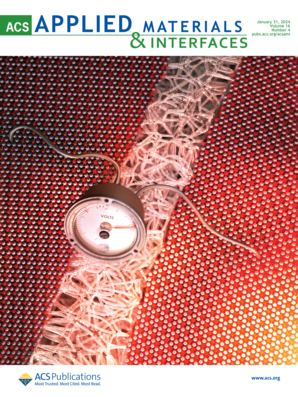
Abstract Image

原子层沉积生长氧化铍薄膜的热输运及其对器件冷却的影响
薄膜氧化铍(BeO)是一种新兴材料,有潜力用作高导热栅极介质和/或大功率电子器件的钝化层。本研究测量了等离子体增强原子层沉积(PEALD)在厚度为25至250 nm的Si衬底上生长的多晶BeO薄膜的热导率和热边界导率。250、113、53和26 nm厚BeO薄膜的面外热导率分别为13.45±1.45、8.7±1.35、7.2±2.1和5±2.2 W m-1 K-1,比传统介质材料(如SiN和SiO2)提高了一个数量级。在室温下,通过BeO/Si界面的测量热边界电导为~ 200 MW m-2 K-1,接近固有界面极限,表明界面热传输主要由弹性声子传输控制。利用5nm厚的BeO金刚石播种,在AlGaN/GaN-on- si外延片上生长了~ 200nm厚的多晶金刚石薄膜,其中充分保留了潜在的AlGaN/GaN异质结构的结构完整性。对集成了顶部多晶金刚石散热片的AlGaN/GaN高电子迁移率晶体管(hemt)的热模拟表明,用BeO取代传统的SiO2钝化成核层有助于将通道温升额外降低5.2%。
本文章由计算机程序翻译,如有差异,请以英文原文为准。
求助全文
约1分钟内获得全文 求助全文
来源期刊
ACS Applied Materials & Interfaces
ACS Applied Materials & Interfaces 工程技术-材料科学:综合
CiteScore
16.00
自引率
6.30%
发文量
4978
审稿时长
1.8 months
期刊介绍: ACS Applied Materials & Interfaces is a leading interdisciplinary journal that brings together chemists, engineers, physicists, and biologists to explore the development and utilization of newly-discovered materials and interfacial processes for specific applications. Our journal has experienced remarkable growth since its establishment in 2009, both in terms of the number of articles published and the impact of the research showcased. We are proud to foster a truly global community, with the majority of published articles originating from outside the United States, reflecting the rapid growth of applied research worldwide.

×
引用
GB/T 7714-2015
复制
MLA
复制
APA
复制
导出至
BibTeX EndNote RefMan NoteFirst NoteExpress
×
提示
您的信息不完整,为了账户安全,请先补充。
现在去补充
×
提示
您因"违规操作"
具体请查看互助需知
我知道了
×
提示
确定
请完成安全验证×
copy
已复制链接
快去分享给好友吧!
我知道了
右上角分享
点击右上角分享
0
联系我们:info@booksci.cn Book学术提供免费学术资源搜索服务,方便国内外学者检索中英文文献。致力于提供最便捷和优质的服务体验。 Copyright © 2023 布克学术 All rights reserved.
京ICP备2023020795号-1
ghs 京公网安备 11010802042870号
Book学术文献互助
Book学术文献互助群
群 号:604180095
Book学术官方微信
小红书


