{"title":"Self-Assembled Metal–Insulator–Metal Tunnel Junctions","authors":"Damon B. Farmer","doi":"10.1021/acsaelm.6c01224","DOIUrl":null,"url":null,"abstract":"<p>Metal–insulator–metal (MIM) tunnel junctions have various applications in microelectronics. As a core building block within this space, these simple structures are fabricated using conventional patterning, deposition, and etching techniques. As such, MIM devices are subject to the inherent limitations and undesirable byproducts of these techniques. Herein, an alternative approach to MIM tunnel junction fabrication is presented, in which classical patterning is used in conjunction with bottom-up, self-assembly to form these structures. Area-selective deposition is utilized to grow encroaching electrodes that terminate at their meeting point to make junctions. The resulting resistances of these junctions are found to be independent of their initial spacing, an indication of self-limited growth. Temperature dependence of these resistances and the behavior of these devices upon annealing indicate electronic tunneling as the dominant transport mechanism. Analysis of these properties is used to estimate barrier thicknesses and conclude that steric effects are the likely reason for self-limitation.</p>","PeriodicalId":3,"journal":{"name":"ACS Applied Electronic Materials","volume":"8 19","pages":"8482–8489"},"PeriodicalIF":4.7000,"publicationDate":"2026-10-13","publicationTypes":"Journal Article","fieldsOfStudy":null,"isOpenAccess":false,"openAccessPdf":"","citationCount":"0","resultStr":null,"platform":"Semanticscholar","paperid":null,"PeriodicalName":"ACS Applied Electronic Materials","FirstCategoryId":"88","ListUrlMain":"https://pubs.acs.org/doi/10.1021/acsaelm.6c01224","RegionNum":3,"RegionCategory":"材料科学","ArticlePicture":[],"TitleCN":null,"AbstractTextCN":null,"PMCID":null,"EPubDate":"2026/9/25 0:00:00","PubModel":"Epub","JCR":"Q1","JCRName":"ENGINEERING, ELECTRICAL & ELECTRONIC","Score":null,"Total":0}
引用次数: 0
Abstract
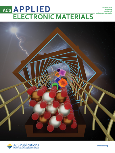
Metal–insulator–metal (MIM) tunnel junctions have various applications in microelectronics. As a core building block within this space, these simple structures are fabricated using conventional patterning, deposition, and etching techniques. As such, MIM devices are subject to the inherent limitations and undesirable byproducts of these techniques. Herein, an alternative approach to MIM tunnel junction fabrication is presented, in which classical patterning is used in conjunction with bottom-up, self-assembly to form these structures. Area-selective deposition is utilized to grow encroaching electrodes that terminate at their meeting point to make junctions. The resulting resistances of these junctions are found to be independent of their initial spacing, an indication of self-limited growth. Temperature dependence of these resistances and the behavior of these devices upon annealing indicate electronic tunneling as the dominant transport mechanism. Analysis of these properties is used to estimate barrier thicknesses and conclude that steric effects are the likely reason for self-limitation.
期刊介绍:
ACS Applied Electronic Materials is an interdisciplinary journal publishing original research covering all aspects of electronic materials. The journal is devoted to reports of new and original experimental and theoretical research of an applied nature that integrate knowledge in the areas of materials science, engineering, optics, physics, and chemistry into important applications of electronic materials. Sample research topics that span the journal's scope are inorganic, organic, ionic and polymeric materials with properties that include conducting, semiconducting, superconducting, insulating, dielectric, magnetic, optoelectronic, piezoelectric, ferroelectric and thermoelectric.
Indexed/Abstracted:
Web of Science SCIE
Scopus
CAS
INSPEC
Portico

 求助内容:
 应助结果提醒方式:


 京公网安备 11010802042870号


