{"title":"Cu-Doped Ga2O3 Thin Films Enabling High-Performance p-Type Solar-Blind Photodetectors","authors":"Moumita Pradhan, Shivani, Ashish Sharma, Chaitanya B. Auti, Pradeep Kumar, Vivekanand Shukla, Mukesh Kumar","doi":"10.1021/acsaelm.6c00668","DOIUrl":null,"url":null,"abstract":"<p>Low hole mobility, strong hole trapping, and self-compensation effects limit the achievement of stable p-type conductivity in the β-Ga<sub>2</sub>O<sub>3</sub> semiconductor, thereby inhibiting its application in advanced electronic devices. From a theoretical standpoint, the relatively flat nature of the valence band maximum (VBM) with dominant oxygen vacancy-related donor states constitutes a major bottleneck that intrinsically drives the material toward n-type conductivity. In this study, we successfully achieved p-type conductivity in gallium oxide thin films using copper doping. The introduction of controlled Cu as an acceptor dopant using RF magnetron sputtering into the Ga<sub>2</sub>O<sub>3</sub> film facilitates bipolar transport by creating an acceptor impurity level near the valence band maximum (VBM), resulting in conductivity modulation. X-ray photoelectron spectroscopy (XPS) and capacitance–voltage (<em>C</em>–<em>V</em>) measurements provide evidence of p-type conduction with a high hole concentration on the order of 10<sup>19</sup>cm<sup>–3</sup>. The positive Seebeck coefficient (<em>S</em>) further confirms hole-dominated electrical transport. Moreover, theoretical analysis reveals that the Cu-induced localized states near the VBM predominantly originate from Cu-d states hybridized with O-p states, indicating strong local Cu–O interactions at the octahedral sites and providing microscopic insight into the experimentally observed modulation of electrical conductivity. Finally, a solar-blind photodetector was fabricated using optimized copper-doped p-type gallium oxide thin films. The fabricated device demonstrates remarkably high performance with a photo-to-dark current ratio (PDCR) of 157.33 ± 0.88, responsivity of 806.88 ± 20.55 A/W, external quantum efficiency of (4.01 ± 0.10) × 10<sup>5</sup>%, noise-equivalent power of (1.88 ± 0.01) × 10<sup>–</sup><sup>13</sup> W Hz<sup>–</sup><sup>1/2</sup>, and a specific detectivity of (2.58 ± 0.05) × 10<sup>12</sup> Jones at 250 nm with a moderate bias of 5 V at a 1 Hz frequency, demonstrating consistent performance across five nominally identical devices. These findings show that the interfacial electrostatics and charge-transport mechanisms in Ga<sub>2</sub>O<sub>3</sub> Schottky devices are efficiently tuned by regulated Cu inclusion, offering insights for enhancing ultra-wide-bandgap oxide-related devices.</p>","PeriodicalId":3,"journal":{"name":"ACS Applied Electronic Materials","volume":"8 19","pages":"8344–8361"},"PeriodicalIF":4.7000,"publicationDate":"2026-10-13","publicationTypes":"Journal Article","fieldsOfStudy":null,"isOpenAccess":false,"openAccessPdf":"","citationCount":"0","resultStr":null,"platform":"Semanticscholar","paperid":null,"PeriodicalName":"ACS Applied Electronic Materials","FirstCategoryId":"88","ListUrlMain":"https://pubs.acs.org/doi/10.1021/acsaelm.6c00668","RegionNum":3,"RegionCategory":"材料科学","ArticlePicture":[],"TitleCN":null,"AbstractTextCN":null,"PMCID":null,"EPubDate":"2026/10/1 0:00:00","PubModel":"Epub","JCR":"Q1","JCRName":"ENGINEERING, ELECTRICAL & ELECTRONIC","Score":null,"Total":0}
引用次数: 0
Abstract
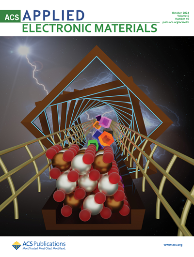
Low hole mobility, strong hole trapping, and self-compensation effects limit the achievement of stable p-type conductivity in the β-Ga2O3 semiconductor, thereby inhibiting its application in advanced electronic devices. From a theoretical standpoint, the relatively flat nature of the valence band maximum (VBM) with dominant oxygen vacancy-related donor states constitutes a major bottleneck that intrinsically drives the material toward n-type conductivity. In this study, we successfully achieved p-type conductivity in gallium oxide thin films using copper doping. The introduction of controlled Cu as an acceptor dopant using RF magnetron sputtering into the Ga2O3 film facilitates bipolar transport by creating an acceptor impurity level near the valence band maximum (VBM), resulting in conductivity modulation. X-ray photoelectron spectroscopy (XPS) and capacitance–voltage (C–V) measurements provide evidence of p-type conduction with a high hole concentration on the order of 1019cm–3. The positive Seebeck coefficient (S) further confirms hole-dominated electrical transport. Moreover, theoretical analysis reveals that the Cu-induced localized states near the VBM predominantly originate from Cu-d states hybridized with O-p states, indicating strong local Cu–O interactions at the octahedral sites and providing microscopic insight into the experimentally observed modulation of electrical conductivity. Finally, a solar-blind photodetector was fabricated using optimized copper-doped p-type gallium oxide thin films. The fabricated device demonstrates remarkably high performance with a photo-to-dark current ratio (PDCR) of 157.33 ± 0.88, responsivity of 806.88 ± 20.55 A/W, external quantum efficiency of (4.01 ± 0.10) × 105%, noise-equivalent power of (1.88 ± 0.01) × 10–13 W Hz–1/2, and a specific detectivity of (2.58 ± 0.05) × 1012 Jones at 250 nm with a moderate bias of 5 V at a 1 Hz frequency, demonstrating consistent performance across five nominally identical devices. These findings show that the interfacial electrostatics and charge-transport mechanisms in Ga2O3 Schottky devices are efficiently tuned by regulated Cu inclusion, offering insights for enhancing ultra-wide-bandgap oxide-related devices.
期刊介绍:
ACS Applied Electronic Materials is an interdisciplinary journal publishing original research covering all aspects of electronic materials. The journal is devoted to reports of new and original experimental and theoretical research of an applied nature that integrate knowledge in the areas of materials science, engineering, optics, physics, and chemistry into important applications of electronic materials. Sample research topics that span the journal's scope are inorganic, organic, ionic and polymeric materials with properties that include conducting, semiconducting, superconducting, insulating, dielectric, magnetic, optoelectronic, piezoelectric, ferroelectric and thermoelectric.
Indexed/Abstracted:
Web of Science SCIE
Scopus
CAS
INSPEC
Portico

 求助内容:
 应助结果提醒方式:


 京公网安备 11010802042870号


