
Programmable Multidimensional Diffraction Engineering via an Optically Addressed Nested Fourier Metasurface
IF 6.8
2区 物理与天体物理
Q1 MATERIALS SCIENCE, MULTIDISCIPLINARY
引用次数: 0
Abstract
ABSTRACT Free‐space optical routing and programmable Fourier optical processing are promising for next‐generation photonic information systems. Here, we propose an optically addressed nested Fourier metasurface (OA‐NFM) platform for dynamically switchable, multidimensional optical routing and diffraction‐channel engineering without dense electrical interconnects. By integrating a Fourier‐coefficient‐based inverse‐design method with a nested Fourier metasurface architecture, the proposed platform enables simultaneous control of diffraction channels and polarization states. By spatially multiplexing Fourier‐engineered mode regions within nested supercells and activating them through digital light processing (DLP)‐based optical addressing, the OA‐NFM achieves programmable momentum‐space redistribution, sideband clustering, and angular‐channel engineering via controllable superlattice diffraction. The local Fourier mode defines the target diffraction response, while the global nested array factor controls the angular distribution of clustered sidebands. Simulations show that individually optimized modes achieve diffraction efficiencies up to 45% with polarization fidelities above 0.99. The OA‐NFM achieves diffraction efficiencies up to 37% within the ± 1.1° receiver window, excluding losses from the DMD and projection optics. NRZ‐OOK simulations confirm BERs below the hard‐decision FEC threshold (10 −3 ) at 25 Gbps across the 1500–1600 nm band. This work demonstrates a promising platform for optical switching, free‐space routing, and multidimensional photonic information processing.基于光学寻址嵌套傅立叶超表面的可编程多维衍射工程
自由空间光路由和可编程傅立叶光处理在下一代光子信息系统中很有前途。在这里,我们提出了一个光学寻址嵌套傅立叶超表面(OA‐NFM)平台,用于动态切换,多维光路由和衍射通道工程,而无需密集的电气互连。通过将基于傅里叶系数的反设计方法与嵌套的傅里叶超表面结构相结合,该平台可以同时控制衍射通道和偏振态。通过在嵌套超单元内对傅里叶工程模式区域进行空间复用,并通过基于数字光处理(DLP)的光学寻址激活它们,OA - NFM实现了可编程的动量-空间再分配、边带聚类和通过可控超晶格衍射实现的角通道工程。局部傅里叶模式定义目标衍射响应,而全局嵌套阵列因子控制聚集边带的角分布。仿真结果表明,单个优化模式的衍射效率可达45%,偏振保真度高于0.99。OA‐NFM在±1.1°的接收窗口内实现了高达37%的衍射效率,不包括DMD和投影光学器件的损耗。NRZ‐OOK模拟证实,在1500 - 1600nm频段的25gbps下,ber低于硬决策FEC阈值(10−3)。这项工作为光交换、自由空间路由和多维光子信息处理展示了一个有前途的平台。
本文章由计算机程序翻译,如有差异,请以英文原文为准。
求助全文
约1分钟内获得全文
求助全文
来源期刊
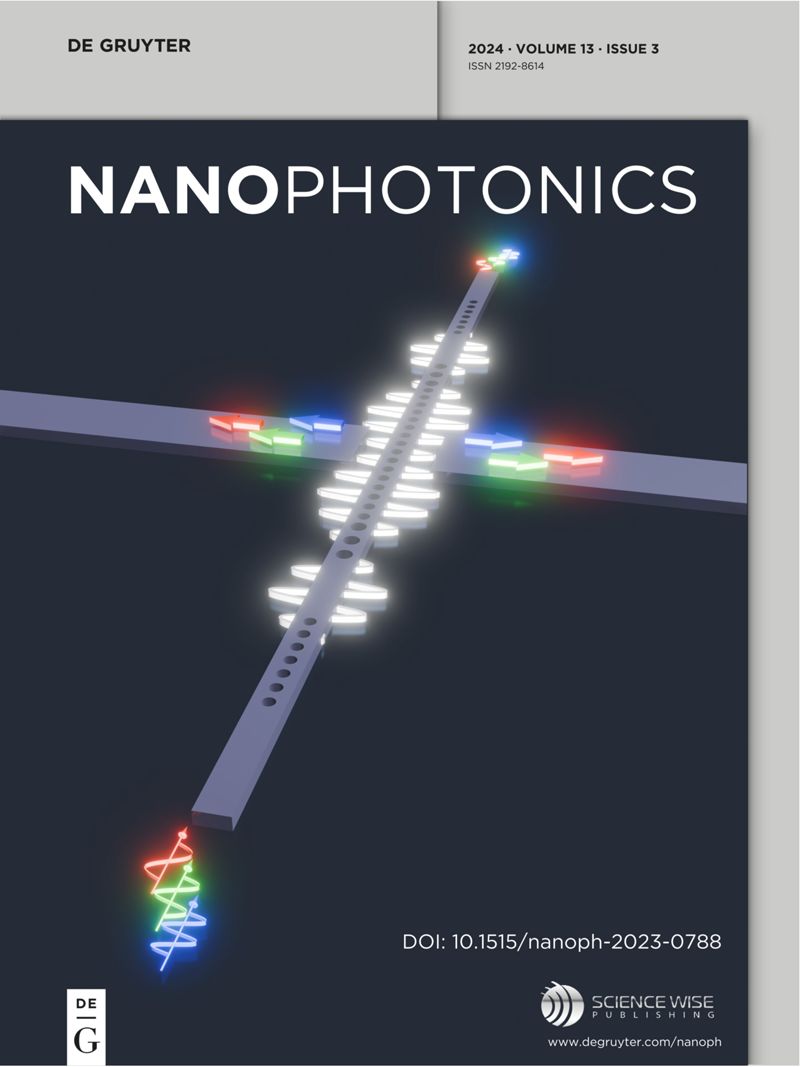
Nanophotonics
NANOSCIENCE & NANOTECHNOLOGY-MATERIALS SCIENCE, MULTIDISCIPLINARY
CiteScore
13.50
自引率
6.70%
发文量
358
审稿时长
7 weeks
期刊介绍:
Nanophotonics, published in collaboration with Sciencewise, is a prestigious journal that showcases recent international research results, notable advancements in the field, and innovative applications. It is regarded as one of the leading publications in the realm of nanophotonics and encompasses a range of article types including research articles, selectively invited reviews, letters, and perspectives.
The journal specifically delves into the study of photon interaction with nano-structures, such as carbon nano-tubes, nano metal particles, nano crystals, semiconductor nano dots, photonic crystals, tissue, and DNA. It offers comprehensive coverage of the most up-to-date discoveries, making it an essential resource for physicists, engineers, and material scientists.
 求助内容:
 应助结果提醒方式:


 京公网安备 11010802042870号


