{"title":"Bias-Tunable Dual-Mode Optoelectronic Device Based on a SiC/β-Ga2O3 Heterojunction for Photodetection and Optical Synapse","authors":"Zhixin Lin, Xiannian Shi, Meijie Yin, Jiao Xu, Teng Yun, Dengji Guo, Xujin Wang, Sudong Wu","doi":"10.1021/acsaom.6c00386","DOIUrl":null,"url":null,"abstract":"<p>Integrating ultraviolet photodetection\r\nand persistent optical memory\r\nin a single compact device is challenging because the two functions\r\nrequire contrasting carrier-recovery dynamics. Here, we demonstrate\r\nbias-only reconfiguration of a two-terminal SiC/β-Ga<sub>2</sub>O<sub>3</sub> heterojunction between a photodetector-like mode and\r\nan optoelectronic-synapse mode. An approximately 27 nm Ga<sub>2</sub>O<sub>3</sub> layer was deposited on n-type 4H-SiC by plasma-enhanced\r\natomic layer deposition and crystallized into β-Ga<sub>2</sub>O<sub>3</sub> by postdeposition annealing at 700 °C. At bias\r\nvoltage <em>V</em><sub>D</sub> = 0.1 V under 254 nm illumination\r\nat 30 μW/cm<sup>2</sup>, the device yields a responsivity (<em>R</em>) of 3.8 A/W, a photocurrent-to-dark-current ratio (<em>PDCR</em>) of 24, an external quantum efficiency (<em>EQE</em>) of 1.85 × 10<sup>3</sup>%, and a shot-noise-limited specific\r\ndetectivity (<em>D*</em>) of 3.0 × 10<sup>12</sup> Jones.\r\nAt the same irradiance, the responsivity ratio <em>R</em><sub>254</sub>/<em>R</em><sub>380</sub> reaches 8.98, while the\r\nvisible-light response remains at the experimental background level,\r\ncorresponding to a conservative lower bound of <em>R</em><sub>254</sub>/<em>R</em><sub>500</sub> > 100. At <em>V</em><sub>D</sub> ≥ 1.5 V, persistent photoconductivity dominates,\r\nenabling a paired-pulse-facilitation index of 156%, pulse-interval-controlled\r\nshort-term-to-long-term memory conversion, and associative learning\r\nunder dual-wavelength UV stimulation. Control-device, transient, structural,\r\nand spectroscopic results support a working model in which a weak\r\ntype-II alignment facilitates bias-regulated interfacial electron\r\ntransfer and defect-state recapture. These results establish a low-voltage,\r\ngate-free route toward compact, reconfigurable deep-UV sensors and\r\nneuromorphic vision devices.</p>","PeriodicalId":29803,"journal":{"name":"ACS Applied Optical Materials","volume":"4 9","pages":"2652–2664"},"PeriodicalIF":3.4000,"publicationDate":"2026-09-25","publicationTypes":"Journal Article","fieldsOfStudy":null,"isOpenAccess":false,"openAccessPdf":"","citationCount":"0","resultStr":null,"platform":"Semanticscholar","paperid":null,"PeriodicalName":"ACS Applied Optical Materials","FirstCategoryId":"1085","ListUrlMain":"https://pubs.acs.org/doi/10.1021/acsaom.6c00386","RegionNum":0,"RegionCategory":null,"ArticlePicture":[],"TitleCN":null,"AbstractTextCN":null,"PMCID":null,"EPubDate":"2026/9/7 0:00:00","PubModel":"Epub","JCR":"","JCRName":"","Score":null,"Total":0}
引用次数: 0
Abstract
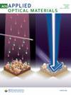
Integrating ultraviolet photodetection
and persistent optical memory
in a single compact device is challenging because the two functions
require contrasting carrier-recovery dynamics. Here, we demonstrate
bias-only reconfiguration of a two-terminal SiC/β-Ga2O3 heterojunction between a photodetector-like mode and
an optoelectronic-synapse mode. An approximately 27 nm Ga2O3 layer was deposited on n-type 4H-SiC by plasma-enhanced
atomic layer deposition and crystallized into β-Ga2O3 by postdeposition annealing at 700 °C. At bias
voltage VD = 0.1 V under 254 nm illumination
at 30 μW/cm2, the device yields a responsivity (R) of 3.8 A/W, a photocurrent-to-dark-current ratio (PDCR) of 24, an external quantum efficiency (EQE) of 1.85 × 10³%, and a shot-noise-limited specific
detectivity (D*) of 3.0 × 10¹² Jones.
At the same irradiance, the responsivity ratio R254/R380 reaches 8.98, while the
visible-light response remains at the experimental background level,
corresponding to a conservative lower bound of R254/R500 > 100. At VD ≥ 1.5 V, persistent photoconductivity dominates,
enabling a paired-pulse-facilitation index of 156%, pulse-interval-controlled
short-term-to-long-term memory conversion, and associative learning
under dual-wavelength UV stimulation. Control-device, transient, structural,
and spectroscopic results support a working model in which a weak
type-II alignment facilitates bias-regulated interfacial electron
transfer and defect-state recapture. These results establish a low-voltage,
gate-free route toward compact, reconfigurable deep-UV sensors and
neuromorphic vision devices.
期刊介绍:
ACS Applied Optical Materials is an international and interdisciplinary forum to publish original experimental and theoretical including simulation and modeling research in optical materials complementing the ACS Applied Materials portfolio. With a focus on innovative applications ACS Applied Optical Materials also complements and expands the scope of existing ACS publications that focus on fundamental aspects of the interaction between light and matter in materials science including ACS Photonics Macromolecules Journal of Physical Chemistry C ACS Nano and Nano Letters.The scope of ACS Applied Optical Materials includes high quality research of an applied nature that integrates knowledge in materials science chemistry physics optical science and engineering.

 求助内容:
 应助结果提醒方式:


 京公网安备 11010802042870号


