Víctor Gonzalez-Morote, Marianna Sledzinska, Arkadiusz P. Gertych, Syed Hassan Abbas Jaffery, Mariusz Zdrojek, Daniel Navarro-Urrios
{"title":"Evanescent Absorption Spectroscopy of Transition Metal Dichalcogenide Materials Using Guided Photoluminescence in Si3N4 Photonic Waveguides","authors":"Víctor Gonzalez-Morote, Marianna Sledzinska, Arkadiusz P. Gertych, Syed Hassan Abbas Jaffery, Mariusz Zdrojek, Daniel Navarro-Urrios","doi":"10.1021/acsaom.6c00415","DOIUrl":null,"url":null,"abstract":"<p>On-chip integration of two-dimensional transition metal\r\ndichalcogenides\r\n(TMDs) with photonic waveguides underpins a growing class of compact\r\noptoelectronic and sensing devices, whose performance depends on the\r\noptical absorption of the two-dimensional (2D) material in this integrated\r\nenvironment. We demonstrate a source-free, on-chip evanescent absorption\r\nspectroscopy of MoS<sub>2</sub> and WS<sub>2</sub> flakes integrated\r\non Si<sub>3</sub>N<sub>4</sub> waveguides, in which the broadband\r\ndefect-related photoluminescence of the Si<sub>3</sub>N<sub>4</sub> core itself acts as the internal probe. Light generated inside the\r\ncore propagates under the TMD flake and is spectrally attenuated by\r\nevanescent interaction with the 2D material, and normalizing the transmitted\r\nspectrum to a reference waveguide without TMD yields the energy-dependent\r\nabsorption response without requiring an external broadband probe.\r\nThe extracted guided absorption agrees with Raman and local micro-photoluminescence\r\ncharacterization and resolves differences between spatially uniform\r\nand non-uniform flakes. A complementary top-pumping scheme recovers\r\nguided WS<sub>2</sub> photoluminescence, whose spectral reshaping\r\nduring propagation is quantitatively reproduced by the measured absorption.\r\nThis source-free platform qualifies 2D materials in their integrated\r\nphotonic environment and provides a direct route toward waveguide-integrated\r\nTMD photodetectors and sensors.</p>","PeriodicalId":29803,"journal":{"name":"ACS Applied Optical Materials","volume":"4 9","pages":"2765–2773"},"PeriodicalIF":3.4000,"publicationDate":"2026-09-25","publicationTypes":"Journal Article","fieldsOfStudy":null,"isOpenAccess":false,"openAccessPdf":"","citationCount":"0","resultStr":null,"platform":"Semanticscholar","paperid":null,"PeriodicalName":"ACS Applied Optical Materials","FirstCategoryId":"1085","ListUrlMain":"https://pubs.acs.org/doi/10.1021/acsaom.6c00415","RegionNum":0,"RegionCategory":null,"ArticlePicture":[],"TitleCN":null,"AbstractTextCN":null,"PMCID":null,"EPubDate":"2026/9/10 0:00:00","PubModel":"Epub","JCR":"","JCRName":"","Score":null,"Total":0}
引用次数: 0
Abstract
On-chip integration of two-dimensional transition metal
dichalcogenides
(TMDs) with photonic waveguides underpins a growing class of compact
optoelectronic and sensing devices, whose performance depends on the
optical absorption of the two-dimensional (2D) material in this integrated
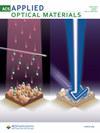
environment. We demonstrate a source-free, on-chip evanescent absorption
spectroscopy of MoS2 and WS2 flakes integrated
on Si3N4 waveguides, in which the broadband
defect-related photoluminescence of the Si3N4 core itself acts as the internal probe. Light generated inside the
core propagates under the TMD flake and is spectrally attenuated by
evanescent interaction with the 2D material, and normalizing the transmitted
spectrum to a reference waveguide without TMD yields the energy-dependent
absorption response without requiring an external broadband probe.
The extracted guided absorption agrees with Raman and local micro-photoluminescence
characterization and resolves differences between spatially uniform
and non-uniform flakes. A complementary top-pumping scheme recovers
guided WS2 photoluminescence, whose spectral reshaping
during propagation is quantitatively reproduced by the measured absorption.
This source-free platform qualifies 2D materials in their integrated
photonic environment and provides a direct route toward waveguide-integrated
TMD photodetectors and sensors.
期刊介绍:
ACS Applied Optical Materials is an international and interdisciplinary forum to publish original experimental and theoretical including simulation and modeling research in optical materials complementing the ACS Applied Materials portfolio. With a focus on innovative applications ACS Applied Optical Materials also complements and expands the scope of existing ACS publications that focus on fundamental aspects of the interaction between light and matter in materials science including ACS Photonics Macromolecules Journal of Physical Chemistry C ACS Nano and Nano Letters.The scope of ACS Applied Optical Materials includes high quality research of an applied nature that integrates knowledge in materials science chemistry physics optical science and engineering.

 求助内容:
 应助结果提醒方式:


 京公网安备 11010802042870号


