{"title":"Enhanced room-temperature thermoelectric power factor of β-Zn4Sb3 thin films via surface roughness optimization","authors":"Avinash Kumar and S.K. Tripathi","doi":"10.1039/D5SE00688K","DOIUrl":null,"url":null,"abstract":"<p >Roughness-induced resistivity and surface scattering components play a vital role in the optimization of charge carrier transport properties in thin film surfaces. In the present work, the effects of surface roughness on thermoelectric (TE) parameters, namely, the Seebeck coefficient (<em>S</em>), electrical conductivity (<em>σ</em>) and power factor (PF) are investigated. The melt quenching method was employed for the synthesis of β-Zn<small><sub>4</sub></small>Sb<small><sub>3</sub></small>. Thin films of various thicknesses ranging from 69 nm to 363 nm were deposited using a thermal evaporation process, which resulted in variation of the surface roughness from 6.94 nm to 37.51 nm. The maximum <em>S</em> and PF values of 227 μV K<small><sup>−1</sup></small> and 814 μW m<small><sup>−1</sup></small> K<small><sup>−2</sup></small> at room temperature (RT) were obtained for the thin film with a roughness of 28.94 nm, which represented 3.05- and 41.84-fold enhancements, respectively, over the corresponding values for the film with a roughness of 6.94 nm. The enhancement of the <em>S</em> values with increasing roughness was attributed to the introduction of surface energy filtering effects. The maximum <em>σ</em> value of 2.25 × 10<small><sup>4</sup></small> S m<small><sup>−1</sup></small> was obtained for the film with a roughness value of 21.75 nm. The initial increasing trend in the <em>σ</em> values with increasing roughness was attributed to the longer mean free path for the carriers caused by the increased crystallite sizes, and the subsequent decreasing trend was attributed to the increased resistivity, surface scattering and trapping of carriers caused by the dominance of roughness effects. X-ray diffraction (XRD) and Raman spectroscopy were employed to investigate the structural characteristics of the surfaces which revealed enhancement of the crystallite sizes with increasing film thickness. The film thicknesses of the prepared surfaces were determined by cross-sectional field emission scanning electron microscopy (FESEM) and found to be 69 nm, 146 nm, 239 nm, 286 nm and 363 nm. Atomic force microscopy (AFM) was employed to investigate the topographical characteristics and height irregularities of the surfaces. 3D micrographs of the surfaces were constructed, and parameters including roughness, skewness and kurtosis were determined. The surface roughness was consistently enhanced with increasing thickness, which was attributed to the vertical accumulation and growth of larger crystallites. Ultraviolet visible spectroscopy (UV-vis) was employed to investigate the optical properties and estimate the bandgaps. The reduction in the bandgaps was attributed to the reduced confinement effects and enhanced light absorption tendency of rougher surfaces.</p>","PeriodicalId":104,"journal":{"name":"Sustainable Energy & Fuels","volume":" 21","pages":" 5931-5948"},"PeriodicalIF":4.1000,"publicationDate":"2025-09-23","publicationTypes":"Journal Article","fieldsOfStudy":null,"isOpenAccess":false,"openAccessPdf":"","citationCount":"0","resultStr":null,"platform":"Semanticscholar","paperid":null,"PeriodicalName":"Sustainable Energy & Fuels","FirstCategoryId":"88","ListUrlMain":"https://pubs.rsc.org/en/content/articlelanding/2025/se/d5se00688k","RegionNum":3,"RegionCategory":"材料科学","ArticlePicture":[],"TitleCN":null,"AbstractTextCN":null,"PMCID":null,"EPubDate":"","PubModel":"","JCR":"Q2","JCRName":"CHEMISTRY, PHYSICAL","Score":null,"Total":0}
引用次数: 0
Abstract
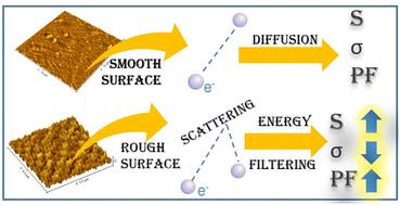
Roughness-induced resistivity and surface scattering components play a vital role in the optimization of charge carrier transport properties in thin film surfaces. In the present work, the effects of surface roughness on thermoelectric (TE) parameters, namely, the Seebeck coefficient (S), electrical conductivity (σ) and power factor (PF) are investigated. The melt quenching method was employed for the synthesis of β-Zn4Sb3. Thin films of various thicknesses ranging from 69 nm to 363 nm were deposited using a thermal evaporation process, which resulted in variation of the surface roughness from 6.94 nm to 37.51 nm. The maximum S and PF values of 227 μV K−1 and 814 μW m−1 K−2 at room temperature (RT) were obtained for the thin film with a roughness of 28.94 nm, which represented 3.05- and 41.84-fold enhancements, respectively, over the corresponding values for the film with a roughness of 6.94 nm. The enhancement of the S values with increasing roughness was attributed to the introduction of surface energy filtering effects. The maximum σ value of 2.25 × 10⁴ S m−1 was obtained for the film with a roughness value of 21.75 nm. The initial increasing trend in the σ values with increasing roughness was attributed to the longer mean free path for the carriers caused by the increased crystallite sizes, and the subsequent decreasing trend was attributed to the increased resistivity, surface scattering and trapping of carriers caused by the dominance of roughness effects. X-ray diffraction (XRD) and Raman spectroscopy were employed to investigate the structural characteristics of the surfaces which revealed enhancement of the crystallite sizes with increasing film thickness. The film thicknesses of the prepared surfaces were determined by cross-sectional field emission scanning electron microscopy (FESEM) and found to be 69 nm, 146 nm, 239 nm, 286 nm and 363 nm. Atomic force microscopy (AFM) was employed to investigate the topographical characteristics and height irregularities of the surfaces. 3D micrographs of the surfaces were constructed, and parameters including roughness, skewness and kurtosis were determined. The surface roughness was consistently enhanced with increasing thickness, which was attributed to the vertical accumulation and growth of larger crystallites. Ultraviolet visible spectroscopy (UV-vis) was employed to investigate the optical properties and estimate the bandgaps. The reduction in the bandgaps was attributed to the reduced confinement effects and enhanced light absorption tendency of rougher surfaces.
期刊介绍:
Sustainable Energy & Fuels will publish research that contributes to the development of sustainable energy technologies with a particular emphasis on new and next-generation technologies.
 求助内容:
求助内容: 应助结果提醒方式:


