Low-Voltage Enhancement-Mode p-Type SnO TFTs enabled by Surface Passivation and High-κ Dielectric Integration
IF 6.3
2区 材料科学
Q2 CHEMISTRY, PHYSICAL
引用次数: 0
Abstract
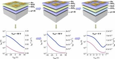
Tin monoxide (SnO), with its high theoretical hole mobility, holds great promise as a p-type semiconductor for complementary metal-oxide semiconductor (CMOS) thin-film transistors (TFTs). However, its low thermal stability and tendency to oxidize into n-type SnO2 have hindered practical device fabrication. Additionally, most reported SnO-TFTs operate in depletion mode and utilize low-κ SiO2 gate dielectrics, resulting in high static power consumption and operating voltages. In this work, we systematically investigate the electrical evolution of p-type SnO films and TFTs by tuning the oxygen partial pressure (Opp) and annealing temperature. We demonstrate that an optimal Opp of 5% combined with annealing at 250 °C effectively suppresses the transformation of p-type SnO into n-type SnO2, while yielding high device performance with a saturation mobility of 3.06 cm2/Vs, an on/off current ratio of 7.15 × 10², a threshold voltage of 18.41 V, and a subthreshold swing of 19.72 V/dec. Moreover, passivating the SnO film with a thin SiO2 layer increases the channel resistance due to the added resistive path and decreases the carrier concentration by partially screening the gate electric field. This electrostatic modulation converts the TFT operation from depletion mode to enhancement mode, reducing static power dissipation and shifting the threshold voltage to -0.17 V. Finally, replacing the conventional 300 nm SiO2 gate dielectric with a solution-processed 30 nm high-κ ZrO2 layer significantly enhances the gate capacitance. This substitution reduces the operating voltages from VGS = -50 V and VDS = -50 V to VGS = -5 V and VDS = -5 V. These findings highlight the importance of synergistic control over the channel, dielectric, and interface engineering to achieve high-performance, low-power p-type SnO TFTs, opening new possibilities for advanced and energy-efficient electronic applications.
表面钝化和高κ介电积分实现的低压增强模式p型SnO tft
一氧化锡(SnO)具有较高的理论空穴迁移率,作为互补金属氧化物半导体(CMOS)薄膜晶体管(TFTs)的p型半导体具有很大的前景。然而,它的低热稳定性和氧化成n型SnO2的倾向阻碍了实际器件的制造。此外,大多数报道的sno - tft在耗尽模式下工作,并利用低κ SiO2栅极介质,导致高静态功耗和工作电压。在这项工作中,我们通过调整氧分压(Opp)和退火温度,系统地研究了p型SnO薄膜和tft的电演化。我们证明,在250 °C下,5%的最佳Opp结合退火有效地抑制了p型SnO2向n型SnO2的转变,同时获得了高的器件性能,饱和迁移率为3.06 cm2/Vs,通/关电流比为7.15 × 102,阈值电压为18.41 V,亚阈值摆振幅为19.72 V/dec。此外,用薄SiO2层钝化SnO膜由于增加了电阻路径而增加了通道电阻,并通过部分屏蔽栅极电场而降低了载流子浓度。这种静电调制将TFT工作从耗尽模式转换为增强模式,降低了静态功耗并将阈值电压移至-0.17 V。最后,用溶液处理的30 nm高κ ZrO2层取代传统的300 nm SiO2栅极介质,显著提高了栅极电容。这种替代降低了操作电压从vg = -50 V和VDS = -50 vg V = 5 V和VDS = 5 V。这些发现强调了通道、介电介质和界面工程协同控制的重要性,以实现高性能、低功耗的p型SnO tft,为先进和节能的电子应用开辟了新的可能性。
本文章由计算机程序翻译,如有差异,请以英文原文为准。
求助全文
约1分钟内获得全文
求助全文
来源期刊
Journal of Alloys and Compounds
工程技术-材料科学:综合
CiteScore
11.10
自引率
14.50%
发文量
5146
审稿时长
67 days
期刊介绍:
The Journal of Alloys and Compounds is intended to serve as an international medium for the publication of work on solid materials comprising compounds as well as alloys. Its great strength lies in the diversity of discipline which it encompasses, drawing together results from materials science, solid-state chemistry and physics.
 求助内容:
求助内容: 应助结果提醒方式:


