Direct Formation of Stable 1T′ Molybdenum Telluride (MoTe2) by Laser Annealing Processes as Robust Contacts for High-Performance Molybdenum Disulfide (MoS2) Field Effect Transistors
IF 8.2
2区 材料科学
Q1 MATERIALS SCIENCE, MULTIDISCIPLINARY
引用次数: 0
Abstract
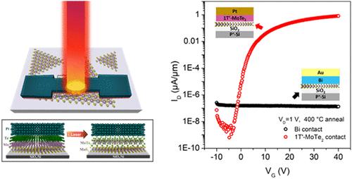
Semimetals, with their low density of states near the Fermi level, effectively suppress metal-induced gap states, enabling near-zero Schottky barrier heights in two-dimensional (2D) field-effect transistors (FETs). However, the low melting point of semimetals (Bi, Sb) limits the applications of 2D FETs at high temperatures. Here, we introduce a robust semimetal contact strategy for high-performance MoS2 FETs, based on continuous-wave laser annealing of elemental metals (Bi, Mo, Pt, W) and tellurium to form metal tellurides. Specifically, the phase of molybdenum telluride (1T′/2H) can be prepared under different laser parameters. In particular, large-area, high-crystallinity films of stable 1T′-MoTe2 can be synthesized uniformly, and source/drain electrodes of 1T′-MoTe2 are formed directly from elemental Mo and Te without damaging the underlying MoS2. Electrical characterization shows that MoS2 FETs with 1T′-MoTe2 contacts match the performance of Bicontacted devices and maintain device uniformity over large areas. Moreover, 1T′-MoTe2 electrodes sustain excellent on/off ratios of ∼108 after an annealing temperature at 400 °C and ∼105 after 500 °C, whereas Bi contacts fail at 400 °C. This laser annealing approach offers a scalable method to fabricate robust electrodes for 2D transistors, paving the way for high-temperature CMOS applications.
用激光退火工艺直接形成稳定的1T '碲化钼(MoTe2)作为高性能二硫化钼(MoS2)场效应晶体管的鲁棒触点
半金属在费米能级附近具有低密度态,可以有效地抑制金属诱导的间隙态,使二维场效应晶体管(fet)中的肖特基势垒高度接近于零。然而,半金属(Bi, Sb)的低熔点限制了二维场效应管在高温下的应用。本文介绍了一种用于高性能MoS2 fet的稳健半金属接触策略,该策略基于连续波激光退火元素金属(Bi, Mo, Pt, W)和碲形成金属碲化物。具体来说,在不同的激光参数下可以制备出1T′/2H的碲化钼相。特别是,可以均匀地合成稳定的大面积、高结晶度的1T ' -MoTe2薄膜,并且1T ' -MoTe2的源极/漏极直接由单质Mo和Te形成,而不会损坏底层的MoS2。电学表征表明,具有1T ' -MoTe2触点的MoS2 fet符合双触点器件的性能,并在大面积上保持器件的均匀性。此外,1T ' -MoTe2电极在400 °C退火温度下和500 °C退火温度下分别保持优良的开/关比为~ 108和~ 105,而Bi触点在400 °C退火温度下失效。这种激光退火方法提供了一种可扩展的方法来制造二维晶体管的坚固电极,为高温CMOS应用铺平了道路。
本文章由计算机程序翻译,如有差异,请以英文原文为准。
求助全文
约1分钟内获得全文
求助全文
来源期刊

ACS Applied Materials & Interfaces
工程技术-材料科学:综合
CiteScore
16.00
自引率
6.30%
发文量
4978
审稿时长
1.8 months
期刊介绍:
ACS Applied Materials & Interfaces is a leading interdisciplinary journal that brings together chemists, engineers, physicists, and biologists to explore the development and utilization of newly-discovered materials and interfacial processes for specific applications. Our journal has experienced remarkable growth since its establishment in 2009, both in terms of the number of articles published and the impact of the research showcased. We are proud to foster a truly global community, with the majority of published articles originating from outside the United States, reflecting the rapid growth of applied research worldwide.
 求助内容:
求助内容: 应助结果提醒方式:


