Transfer method effects on graphene/α-germanium selenide heterostructures: Toward strain and interfacial interactions in bandgap modulation
IF 6.9
2区 材料科学
Q2 CHEMISTRY, PHYSICAL
引用次数: 0
Abstract
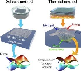
Two-dimensional van der Waals (vdW) materials with an intrinsic bandgap offer promising platforms for integrating graphene into functional heterostructures. In this study, we investigated the relative roles of strain and interfacial interactions in modulating the electronic band structure of graphene within a vdW heterostructure. Our model system is graphene on α-germanium selenide (α-GeSe). By comparing solvent and thermal transfer methods, we explore how fabrication conditions impact the structure and band characteristics of the resulting heterostructures. Scanning probe microscopy and first-principles calculations reveal that solvent-based transfer preserves the substrate integrity and the intrinsic electronic structure of graphene, yielding a novel parallelogram moiré pattern. In contrast, the thermal transfer induces oxidation of Ge and formation of rhombus-shaped etch pits, which locally strain the graphene layer and result in a measurable bandgap. Meanwhile, spatial doping variations are primarily governed by charge transfer effects due to interface interaction. Our findings demonstrate that strain, rather than interlayer coupling, is the dominant mechanism for bandgap modulation in graphene/α-GeSe heterostructure. This work underscores the critical role of transfer techniques in engineering the properties of 2D van der Waals heterojunctions and establishes α-GeSe as a promising, tunable substrate for future graphene-based electronic and optoelectronic applications.
传递方法对石墨烯/α-硒化锗异质结构的影响:带隙调制中的应变和界面相互作用
具有固有带隙的二维范德华(vdW)材料为将石墨烯集成到功能异质结构中提供了有前途的平台。在这项研究中,我们研究了应变和界面相互作用在调制vdW异质结构中石墨烯电子能带结构中的相对作用。我们的模型体系是α-硒化锗(α-GeSe)上的石墨烯。通过比较溶剂和热传递方法,我们探讨了制备条件如何影响所得异质结构的结构和能带特性。扫描探针显微镜和第一性原理计算表明,溶剂基转移保留了基底的完整性和石墨烯的固有电子结构,产生了一种新的平行四边形波纹图。相反,热传递导致Ge氧化并形成菱形蚀刻坑,从而局部应变石墨烯层并导致可测量的带隙。同时,空间掺杂变化主要受界面相互作用引起的电荷转移效应控制。我们的研究结果表明,应变而不是层间耦合是石墨烯/α-GeSe异质结构中带隙调制的主要机制。这项工作强调了转移技术在工程二维范德华异质结特性中的关键作用,并确立了α-GeSe作为未来基于石墨烯的电子和光电子应用的有前途的可调衬底。
本文章由计算机程序翻译,如有差异,请以英文原文为准。
求助全文
约1分钟内获得全文
求助全文
来源期刊

Applied Surface Science
工程技术-材料科学:膜
CiteScore
12.50
自引率
7.50%
发文量
3393
审稿时长
67 days
期刊介绍:
Applied Surface Science covers topics contributing to a better understanding of surfaces, interfaces, nanostructures and their applications. The journal is concerned with scientific research on the atomic and molecular level of material properties determined with specific surface analytical techniques and/or computational methods, as well as the processing of such structures.
 求助内容:
求助内容: 应助结果提醒方式:


