Nanoscale heterojunction indium oxide/molybdenum disulphide field-effect transistor: A cost-effective wafer scale fabrication with improved performance
IF 7.6
Q1 BIOTECHNOLOGY & APPLIED MICROBIOLOGY
引用次数: 0
Abstract
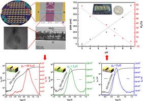
Metal oxide heterojunction thin films are promising building blocks for the fabrication of functional devices in microelectronics, bio-chemical sensors, photovoltaics, and optical displays. However, balancing the large-scale manufacturability with performance, uniformity, and cost-effectiveness remains a significant challenge. Here, we report a wafer-scale fabrication process of bilayer stacks of high-mobility indium oxide and molybdenum disulphide heterojunction thin films and their application for the preparation of high-performance field-effect transistors (FETs). The annealed heterojunction thin film exhibits uniform crystalline structures and good surface roughness across the whole wafer. A simple soft lithography and lift-off process of the heterojunction thin film could produce nanotransistor devices with a remarkable electron mobility enhancement of more than 1100 % compared to indium oxide or molybdenum disulphide single layer devices. The heterojunction FET sensors yielded more than a twofold higher pH sensitivity compared to silicon-based ionic FETs and excellent linearity. These findings coupled with the cost-effective fabrication strategy underscore the potential of indium oxide and molybdenum disulphide heterojunction FET devices.
纳米异质结氧化铟/二硫化钼场效应晶体管:具有改进性能的低成本晶圆级制造
金属氧化物异质结薄膜是制造微电子、生化传感器、光伏和光学显示器等功能器件的有前途的基石。然而,平衡大规模可制造性与性能、一致性和成本效益仍然是一个重大挑战。本文报道了一种高迁移率氧化铟和二硫化钼异质结薄膜双层堆叠的晶圆级制备工艺及其在高性能场效应晶体管(fet)制备中的应用。退火后的异质结薄膜在整个晶圆上具有均匀的晶体结构和良好的表面粗糙度。与氧化铟或二硫化钼单层器件相比,异质结薄膜的简单软光刻和剥离工艺可以生产出电子迁移率提高1100%以上的纳米晶体管器件。与硅基离子FET相比,异质结FET传感器的pH灵敏度提高了两倍以上,线性度也很好。这些发现加上具有成本效益的制造策略,强调了氧化铟和二硫化钼异质结FET器件的潜力。
本文章由计算机程序翻译,如有差异,请以英文原文为准。
求助全文
约1分钟内获得全文
求助全文
来源期刊
Sensors and Actuators Reports
Multiple-
CiteScore
9.60
自引率
0.00%
发文量
60
审稿时长
49 days
期刊介绍:
Sensors and Actuators Reports is a peer-reviewed open access journal launched out from the Sensors and Actuators journal family. Sensors and Actuators Reports is dedicated to publishing new and original works in the field of all type of sensors and actuators, including bio-, chemical-, physical-, and nano- sensors and actuators, which demonstrates significant progress beyond the current state of the art. The journal regularly publishes original research papers, reviews, and short communications.
For research papers and short communications, the journal aims to publish the new and original work supported by experimental results and as such purely theoretical works are not accepted.
 求助内容:
求助内容: 应助结果提醒方式:


