{"title":"Mobility Overestimation in Thin-Film Transistors: Effects of Device Geometry and Fringe Currents","authors":"Soohyun Kim, , , Youngjoon Lee, , , Seokyeon Shin, , , Hyunsoo Kim, , , Hyoseob Shin, , , Hideo Hosono, , , Changwook Jeong*, , and , Junghwan Kim*, ","doi":"10.1021/acsnano.5c11904","DOIUrl":null,"url":null,"abstract":"<p >Amorphous oxide semiconductor-based thin-film transistors (oxide TFTs) were first demonstrated in 2004. These devices offer numerous advantages, including low-temperature processing, high carrier mobility, and ultralow off-current. As a result, oxide TFTs have already been adopted for backplane technologies in modern flat-panel displays. Furthermore, their ultralow off-current has attracted considerable attention for next-generation DRAM applications. However, device reliability remains a critical challenge. In particular, gate bias stress instabilities such as negative bias temperature stress and positive bias temperature stress significantly hinder the advancement of high-mobility oxide TFTs beyond low-temperature polycrystalline silicon (LTPS) technology. Therefore, the evaluation of both field-effect mobility (FEM) and bias stability is essential for oxide TFTs. The absolute value of FEM is especially important when identifying candidate materials to replace LTPS. In this context, we have recently found that incorrect FEM evaluation methods have been widely used in numerous published studies. Such errors have resulted in overestimated FEM values, potentially compromising objective comparisons of materials and fabrication processes. This study clearly demonstrates, through both experimental data and simulation-analytical modeling, how and why FEM overestimation occurs. In particular, we derive a compact analytical expression based on conformal mapping and validate it using TCAD simulations and measurements. This dual-pronged approach establishes a general framework for identifying and correcting mobility overestimation. This study highlights the importance of recognizing and addressing mobility overestimation within the field, and that the proposed FEM evaluation method should be adopted to enable more objective and reliable comparisons.</p>","PeriodicalId":21,"journal":{"name":"ACS Nano","volume":"19 41","pages":"36614–36625"},"PeriodicalIF":16.0000,"publicationDate":"2025-10-10","publicationTypes":"Journal Article","fieldsOfStudy":null,"isOpenAccess":false,"openAccessPdf":"","citationCount":"0","resultStr":null,"platform":"Semanticscholar","paperid":null,"PeriodicalName":"ACS Nano","FirstCategoryId":"88","ListUrlMain":"https://pubs.acs.org/doi/10.1021/acsnano.5c11904","RegionNum":1,"RegionCategory":"材料科学","ArticlePicture":[],"TitleCN":null,"AbstractTextCN":null,"PMCID":null,"EPubDate":"","PubModel":"","JCR":"Q1","JCRName":"CHEMISTRY, MULTIDISCIPLINARY","Score":null,"Total":0}
引用次数: 0
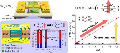
Abstract
Amorphous oxide semiconductor-based thin-film transistors (oxide TFTs) were first demonstrated in 2004. These devices offer numerous advantages, including low-temperature processing, high carrier mobility, and ultralow off-current. As a result, oxide TFTs have already been adopted for backplane technologies in modern flat-panel displays. Furthermore, their ultralow off-current has attracted considerable attention for next-generation DRAM applications. However, device reliability remains a critical challenge. In particular, gate bias stress instabilities such as negative bias temperature stress and positive bias temperature stress significantly hinder the advancement of high-mobility oxide TFTs beyond low-temperature polycrystalline silicon (LTPS) technology. Therefore, the evaluation of both field-effect mobility (FEM) and bias stability is essential for oxide TFTs. The absolute value of FEM is especially important when identifying candidate materials to replace LTPS. In this context, we have recently found that incorrect FEM evaluation methods have been widely used in numerous published studies. Such errors have resulted in overestimated FEM values, potentially compromising objective comparisons of materials and fabrication processes. This study clearly demonstrates, through both experimental data and simulation-analytical modeling, how and why FEM overestimation occurs. In particular, we derive a compact analytical expression based on conformal mapping and validate it using TCAD simulations and measurements. This dual-pronged approach establishes a general framework for identifying and correcting mobility overestimation. This study highlights the importance of recognizing and addressing mobility overestimation within the field, and that the proposed FEM evaluation method should be adopted to enable more objective and reliable comparisons.
期刊介绍:
ACS Nano, published monthly, serves as an international forum for comprehensive articles on nanoscience and nanotechnology research at the intersections of chemistry, biology, materials science, physics, and engineering. The journal fosters communication among scientists in these communities, facilitating collaboration, new research opportunities, and advancements through discoveries. ACS Nano covers synthesis, assembly, characterization, theory, and simulation of nanostructures, nanobiotechnology, nanofabrication, methods and tools for nanoscience and nanotechnology, and self- and directed-assembly. Alongside original research articles, it offers thorough reviews, perspectives on cutting-edge research, and discussions envisioning the future of nanoscience and nanotechnology.


 求助内容:
求助内容: 应助结果提醒方式:


