Lateral Semiconductor–Free-Space Gate Transistors
IF 9.1
1区 材料科学
Q1 CHEMISTRY, MULTIDISCIPLINARY
引用次数: 0
Abstract
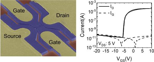
We introduce a novel lateral transistor architecture, the semiconductor–free-space gate transistor (SFGT), in which the conventional solid dielectric is replaced by a semiconductor–free-space gate configuration with sub-100 nm fin channels and dual side gates. This work presents the first demonstration of free-space gating in wide and ultrawide bandgap semiconductors, achieving performance on par with oxide-gated transistors. SFGTs fabricated using β-Ga2O3 exhibit subthreshold slopes below 200 mV/dec, high drain current exceeding 250 mA/mm, hysteresis under 230 mV, ION/IOFF ratios above 106, and breakdown voltages over 500 V. The absence of a solid dielectric layer, combined with the open gate geometry, enables direct access to the gate region for external electric field modulation and threshold voltage tuning, while mitigating the detrimental effects of charges and trap states in conventional dielectrics. These results show the potential of SFGTs for future memory, sensing, and power applications.
横向半导体无空间栅极晶体管
我们介绍了一种新的横向晶体管结构,半导体自由空间栅极晶体管(SFGT),其中传统的固体电介质被具有亚100 nm鳍状通道和双侧栅极的半导体自由空间栅极结构所取代。这项工作首次展示了宽和超宽带隙半导体中的自由空间门控,实现了与氧化门控晶体管相当的性能。用β-Ga2O3制备的SFGTs表现出低于200 mV/dec的亚阈值斜率,超过250 mA/mm的高漏极电流,230 mV以下的迟滞,离子/IOFF比大于106,击穿电压大于500 V。固体介电层的缺失,加上开放式栅极几何结构,使得直接进入栅极区域进行外部电场调制和阈值电压调谐,同时减轻了传统电介质中电荷和陷阱状态的有害影响。这些结果显示了sfgs在未来存储、传感和电源应用方面的潜力。
本文章由计算机程序翻译,如有差异,请以英文原文为准。
求助全文
约1分钟内获得全文
求助全文
来源期刊

Nano Letters
工程技术-材料科学:综合
CiteScore
16.80
自引率
2.80%
发文量
1182
审稿时长
1.4 months
期刊介绍:
Nano Letters serves as a dynamic platform for promptly disseminating original results in fundamental, applied, and emerging research across all facets of nanoscience and nanotechnology. A pivotal criterion for inclusion within Nano Letters is the convergence of at least two different areas or disciplines, ensuring a rich interdisciplinary scope. The journal is dedicated to fostering exploration in diverse areas, including:
- Experimental and theoretical findings on physical, chemical, and biological phenomena at the nanoscale
- Synthesis, characterization, and processing of organic, inorganic, polymer, and hybrid nanomaterials through physical, chemical, and biological methodologies
- Modeling and simulation of synthetic, assembly, and interaction processes
- Realization of integrated nanostructures and nano-engineered devices exhibiting advanced performance
- Applications of nanoscale materials in living and environmental systems
Nano Letters is committed to advancing and showcasing groundbreaking research that intersects various domains, fostering innovation and collaboration in the ever-evolving field of nanoscience and nanotechnology.
 求助内容:
求助内容: 应助结果提醒方式:


