Atomic-level contact formation between LiNbO3 and Si wafers via surface-activated bonding at room temperature

IF 6.9 2区 材料科学 Q2 CHEMISTRY, PHYSICAL
Seigo Murakami, Ryo Takigawa
{"title":"Atomic-level contact formation between LiNbO3 and Si wafers via surface-activated bonding at room temperature","authors":"Seigo Murakami, Ryo Takigawa","doi":"10.1016/j.apsusc.2025.164850","DOIUrl":null,"url":null,"abstract":"Fabrication of high-quality LiNbO<sub>3</sub>/Si interfaces is crucial for the heterogeneous wafer-level integration of single crystal LiNbO<sub>3</sub> and Si. Bonded LiNbO<sub>3</sub>/Si wafers are promising for integrated photonics and RF devices owing to their unique electro-optic, nonlinear-optic, and piezoelectric properties. This study focuses on forming a directly bonded interface between LiNbO<sub>3</sub> and Si wafers using the surface-activated bonding (SAB) method, combined with Ar fast atom beam irradiation at room temperature, and on performing atomic-level analyses of the LiNbO<sub>3</sub>/Si bonded interface and debonded surfaces. The surface activation process produces amorphous Li-deficient LiNbO<sub>3</sub> and Si layers. The SAB method enables LiNbO<sub>3</sub> and Si wafers to form a void-free, atomically bonded interface. Atomic-scale observations and elemental analyses of both the bonded interface and debonded surfaces suggest that the bond strength between LiNbO<sub>3</sub> and Si is primarily determined by the Ar irradiation-induced amorphous LiNbO<sub>3</sub> layer. This study lays a foundation for the future development and mechanistic understanding of SAB for fabricating heterogeneously integrated LiNbO<sub>3</sub> wafers, with potential applications in photonic and RF devices.","PeriodicalId":247,"journal":{"name":"Applied Surface Science","volume":"122 1","pages":""},"PeriodicalIF":6.9000,"publicationDate":"2025-10-09","publicationTypes":"Journal Article","fieldsOfStudy":null,"isOpenAccess":false,"openAccessPdf":"","citationCount":"0","resultStr":null,"platform":"Semanticscholar","paperid":null,"PeriodicalName":"Applied Surface Science","FirstCategoryId":"88","ListUrlMain":"https://doi.org/10.1016/j.apsusc.2025.164850","RegionNum":2,"RegionCategory":"材料科学","ArticlePicture":[],"TitleCN":null,"AbstractTextCN":null,"PMCID":null,"EPubDate":"","PubModel":"","JCR":"Q2","JCRName":"CHEMISTRY, PHYSICAL","Score":null,"Total":0}
引用次数: 0

Abstract

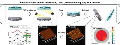
Fabrication of high-quality LiNbO3/Si interfaces is crucial for the heterogeneous wafer-level integration of single crystal LiNbO3 and Si. Bonded LiNbO3/Si wafers are promising for integrated photonics and RF devices owing to their unique electro-optic, nonlinear-optic, and piezoelectric properties. This study focuses on forming a directly bonded interface between LiNbO3 and Si wafers using the surface-activated bonding (SAB) method, combined with Ar fast atom beam irradiation at room temperature, and on performing atomic-level analyses of the LiNbO3/Si bonded interface and debonded surfaces. The surface activation process produces amorphous Li-deficient LiNbO3 and Si layers. The SAB method enables LiNbO3 and Si wafers to form a void-free, atomically bonded interface. Atomic-scale observations and elemental analyses of both the bonded interface and debonded surfaces suggest that the bond strength between LiNbO3 and Si is primarily determined by the Ar irradiation-induced amorphous LiNbO3 layer. This study lays a foundation for the future development and mechanistic understanding of SAB for fabricating heterogeneously integrated LiNbO3 wafers, with potential applications in photonic and RF devices.

Abstract Image

室温下通过表面活化键合形成的LiNbO3和Si晶圆之间的原子级接触
制备高质量的LiNbO3/Si界面是实现单晶LiNbO3和Si非均质片级集成的关键。由于其独特的电光、非线性光学和压电特性,键合LiNbO3/Si晶圆在集成光子学和射频器件中具有广阔的应用前景。本研究的重点是利用表面活化键合(SAB)方法在LiNbO3和Si晶片之间形成直接键合界面,结合室温下的Ar快原子束辐照,并对LiNbO3/Si键合界面和脱键表面进行原子水平分析。表面活化过程产生非晶缺锂LiNbO3和Si层。SAB方法使LiNbO3和Si晶圆形成无空洞的原子键合界面。原子尺度的观察和元素分析表明,LiNbO3与Si之间的结合强度主要是由Ar辐照诱导的非晶态LiNbO3层决定的。该研究为未来SAB的发展和机理理解奠定了基础,为制造异构集成LiNbO3晶圆奠定了基础,在光子和射频器件中具有潜在的应用前景。
本文章由计算机程序翻译,如有差异,请以英文原文为准。
求助全文
约1分钟内获得全文 求助全文
来源期刊
Applied Surface Science
Applied Surface Science 工程技术-材料科学:膜
CiteScore
12.50
自引率
7.50%
发文量
3393
审稿时长
67 days
期刊介绍: Applied Surface Science covers topics contributing to a better understanding of surfaces, interfaces, nanostructures and their applications. The journal is concerned with scientific research on the atomic and molecular level of material properties determined with specific surface analytical techniques and/or computational methods, as well as the processing of such structures.
×
引用
GB/T 7714-2015
复制
MLA
复制
APA
复制
导出至
BibTeX EndNote RefMan NoteFirst NoteExpress
×
提示
您的信息不完整,为了账户安全,请先补充。
现在去补充
×
提示
您因"违规操作"
具体请查看互助需知
我知道了
×
提示
确定
请完成安全验证×
copy
已复制链接
快去分享给好友吧!
我知道了
右上角分享
点击右上角分享
0
联系我们:info@booksci.cn Book学术提供免费学术资源搜索服务,方便国内外学者检索中英文文献。致力于提供最便捷和优质的服务体验。 Copyright © 2023 布克学术 All rights reserved.
京ICP备2023020795号-1
ghs 京公网安备 11010802042870号
Book学术文献互助
Book学术文献互助群
群 号:604180095
Book学术官方微信