Applicability of projection lithography using a gradient-index lens array to patterning of 50–150 micron thick resist
IF 3.7
2区 工程技术
Q2 ENGINEERING, MANUFACTURING
Precision Engineering-Journal of the International Societies for Precision Engineering and Nanotechnology
Pub Date : 2025-09-25
DOI:10.1016/j.precisioneng.2025.09.023
引用次数: 0
Abstract
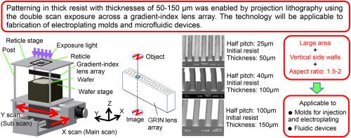
Scan projection lithography using a gradient index lens array as a projection lens is advantageous for printing rough patterns more than 15 μm in large areas at a stretch. In addition to this wonderful performance, it was demonstrated in this paper that patterning in very thick resist films with thicknesses of 50–150 μm was practicable. Since imaging light rays came to a wafer with the maximum inclination angle θ of 12° depending on the property of selected lens array, pattern images formed in the thick resist film with a thickness of t had blurs of b = 2t tan12° = 0.435t at the resist surface. For this reason, the b value became the resolution limit of 1:1 lines-and-spaces patterns printed using a resist with the thickness of t. It was actually demonstrated that the resolution limits for 50- and 100-μm thick resist SU-8 almost corresponded to b. Aspect ratios were also coincided with the estimated value of t/b = 2.35. If the aspect ratios were tolerated to be smaller, patterns with thicknesses of more than 150 μm were printable. In addition, means for improving the patterning performances were discussed. Utilization of a lens array with a smaller inclination angle of imaging light rays, optimization of the exposure-light wavelength, and intentional defocusing of the wafer may be effective.
梯度折射率透镜阵列投影光刻在50-150微米厚抗蚀剂上的适用性
扫描投影光刻技术采用梯度折射率透镜阵列作为投影透镜,有利于大面积连续打印大于15 μm的粗糙图案。除此之外,本文还证明了在厚度为50-150 μm的极厚抗蚀剂薄膜上进行图像化是可行的。由于成像光线到达晶圆时,根据所选透镜阵列的性质,最大倾角θ为12°,因此在厚度为t的厚抗蚀剂薄膜上形成的图案图像在抗蚀剂表面具有b = 2t和12°= 0.435t的模糊。因此,b值成为使用厚度为t的抗蚀剂印刷1:1线条和空间图案的分辨率极限。实际上,50 μm和100 μm厚的抗蚀剂SU-8的分辨率极限几乎与b相对应。纵横比也与t/b = 2.35的估计值相吻合。如果允许宽高比更小,则可以打印厚度超过150 μm的图案。此外,还讨论了提高图案化性能的方法。利用具有较小的成像光线倾斜角的透镜阵列,优化曝光光波长,并有意地使晶圆离焦可能是有效的。
本文章由计算机程序翻译,如有差异,请以英文原文为准。
求助全文
约1分钟内获得全文
求助全文
来源期刊
CiteScore
7.40
自引率
5.60%
发文量
177
审稿时长
46 days
期刊介绍:
Precision Engineering - Journal of the International Societies for Precision Engineering and Nanotechnology is devoted to the multidisciplinary study and practice of high accuracy engineering, metrology, and manufacturing. The journal takes an integrated approach to all subjects related to research, design, manufacture, performance validation, and application of high precision machines, instruments, and components, including fundamental and applied research and development in manufacturing processes, fabrication technology, and advanced measurement science. The scope includes precision-engineered systems and supporting metrology over the full range of length scales, from atom-based nanotechnology and advanced lithographic technology to large-scale systems, including optical and radio telescopes and macrometrology.
 求助内容:
求助内容: 应助结果提醒方式:


