Hasnain Yousuf , Muhammad Quddamah Khokhar , Alamgeer , Mengmeng Chu , Rafi ur Rahman , Maha Nur Aida , Donghyun Oh , Youngkuk Kim , Junsin Yi
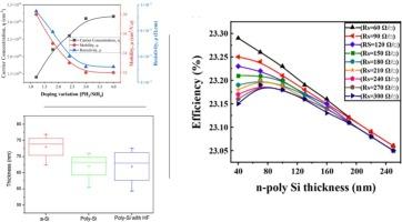
{"title":"Optimizing n+ poly-Si layer doping and plasma treatments for enhanced electrical and thickness uniformity in n-type c-Si wafers","authors":"Hasnain Yousuf , Muhammad Quddamah Khokhar , Alamgeer , Mengmeng Chu , Rafi ur Rahman , Maha Nur Aida , Donghyun Oh , Youngkuk Kim , Junsin Yi","doi":"10.1016/j.rechem.2025.102726","DOIUrl":null,"url":null,"abstract":"<div><div>This study investigates n<sup>+</sup> polycrystalline silicon (poly-Si) layers, focusing on doping concentration and post-deposition treatments, to understand their electrical and structural properties on n-type crystalline silicon wafers. To address challenges in conductivity and film uniformity, the PH<sub>3</sub>/SiH<sub>4</sub> gas ratio (1.2–4.0) was varied during PECVD deposition, followed by high-temperature annealing and selective NH<sub>3</sub> plasma exposure. Amorphous silicon (a-Si:H) was first deposited (on ultrathin SiO<sub>x</sub> for optical-uniformity mapping) and subsequently crystallized into n<sup>+</sup> poly-Si by annealing at 900 °C. Post-treatments (HF dip, NH<sub>3</sub> plasma) were then applied. Increasing dopant ratio raised carrier concentration (<em>n</em>) from 1.4 × 10<sup>20</sup> to 3.16 × 10<sup>20</sup> cm<sup>−3</sup> while decreasing resistivity (<em>ρ</em>) and sheet resistance (<em>R</em><sub><em>s</em></sub>). Zone-dependent variations were evident across the 8-zone PECVD: Zone 4 generally exhibited lower <em>R</em><sub><em>s</em></sub> and higher <em>μ</em>, whereas Zone 8 lagged. Annealing improved crystallinity and electrical uniformity; NH<sub>3</sub> plasma, used here as a surface treatment on the poly-Si layer (not a full passivating-contact stack), produced a small increase in <em>R</em><sub><em>s</em></sub> that indicates the need for further plasma-parameter tuning for uniform electrical outcomes. Raman and ellipsometry confirmed crystallinity (<em>X</em><sub><em>c</em></sub>) and thickness distributions consistent with transport trends. This work focuses on layer-level optimization of n<sup>+</sup> poly-Si; surface passivation quality and contact resistivity (<em>ρ</em><sub><em>c</em></sub>) of complete poly-Si/SiO<sub>x</sub> stacks are not evaluated and will be addressed in future work. For electrical characterization, Hall parameters (<em>n</em>, <em>μ</em>) were extracted using glass-surrogate structures to avoid substrate conduction, and <em>R</em><sub><em>s</em></sub> was measured on wafers by four-point probe. The optimized layers are intended for rear-side electron-selective contacts in conventional n-type TOPCon, where optical penalties are modest; front-side use would require additional thickness minimization and optical re-optimization.</div></div>","PeriodicalId":420,"journal":{"name":"Results in Chemistry","volume":"18 ","pages":"Article 102726"},"PeriodicalIF":4.2000,"publicationDate":"2025-09-19","publicationTypes":"Journal Article","fieldsOfStudy":null,"isOpenAccess":false,"openAccessPdf":"","citationCount":"0","resultStr":null,"platform":"Semanticscholar","paperid":null,"PeriodicalName":"Results in Chemistry","FirstCategoryId":"1085","ListUrlMain":"https://www.sciencedirect.com/science/article/pii/S221171562500709X","RegionNum":0,"RegionCategory":null,"ArticlePicture":[],"TitleCN":null,"AbstractTextCN":null,"PMCID":null,"EPubDate":"","PubModel":"","JCR":"Q2","JCRName":"CHEMISTRY, MULTIDISCIPLINARY","Score":null,"Total":0}
引用次数: 0
Abstract
This study investigates n+ polycrystalline silicon (poly-Si) layers, focusing on doping concentration and post-deposition treatments, to understand their electrical and structural properties on n-type crystalline silicon wafers. To address challenges in conductivity and film uniformity, the PH3/SiH4 gas ratio (1.2–4.0) was varied during PECVD deposition, followed by high-temperature annealing and selective NH3 plasma exposure. Amorphous silicon (a-Si:H) was first deposited (on ultrathin SiOx for optical-uniformity mapping) and subsequently crystallized into n+ poly-Si by annealing at 900 °C. Post-treatments (HF dip, NH3 plasma) were then applied. Increasing dopant ratio raised carrier concentration (n) from 1.4 × 10²⁰ to 3.16 × 1020 cm−3 while decreasing resistivity (ρ) and sheet resistance (Rs). Zone-dependent variations were evident across the 8-zone PECVD: Zone 4 generally exhibited lower Rs and higher μ, whereas Zone 8 lagged. Annealing improved crystallinity and electrical uniformity; NH3 plasma, used here as a surface treatment on the poly-Si layer (not a full passivating-contact stack), produced a small increase in Rs that indicates the need for further plasma-parameter tuning for uniform electrical outcomes. Raman and ellipsometry confirmed crystallinity (Xc) and thickness distributions consistent with transport trends. This work focuses on layer-level optimization of n+ poly-Si; surface passivation quality and contact resistivity (ρc) of complete poly-Si/SiOx stacks are not evaluated and will be addressed in future work. For electrical characterization, Hall parameters (n, μ) were extracted using glass-surrogate structures to avoid substrate conduction, and Rs was measured on wafers by four-point probe. The optimized layers are intended for rear-side electron-selective contacts in conventional n-type TOPCon, where optical penalties are modest; front-side use would require additional thickness minimization and optical re-optimization.

 求助内容:
求助内容: 应助结果提醒方式:


