{"title":"Optimum design of a lateral superjunction considering charge imbalance due to process variations","authors":"Rachita Mohapatra, K. Akshay","doi":"10.1007/s10825-025-02432-0","DOIUrl":null,"url":null,"abstract":"<div><p>Lateral superjunctions (LSJ) are potential candidates for CMOS compatible high voltage devices in next-generation power integrated circuits. The prior works have modeled and developed design guidelines only for an ideal balanced LSJ, i.e., having equal charge in the n- and p-pillars. However, inevitable process variation during fabrication results in charge imbalance, <span>\\({k_{N}}\\)</span>, that yields a breakdown voltage, <span>\\({V_\\textrm{BR}}\\)</span>, significantly lower than the target breakdown voltage, <span>\\({V_\\textrm{BR,target}}\\)</span>. In this work, we use the method of Lagrange multipliers to derive analytical equations for the optimum pillar parameters of an LSJ; these parameters yield the minimum specific ON-resistance, <span>\\({R_\\textrm{ONSP}}\\)</span>, for a <span>\\({V_\\textrm{BR,target}}\\)</span> and <span>\\({k_{N}}\\)</span>. The analytical solutions are verified using well-calibrated TCAD simulations for 0.1–1 kV Si LSJs and 1–10 kV 4H-SiC LSJs for <span>\\({k_{N}}\\)</span> from 0.05 to 0.30 (signifying 5 to 30% imbalance between the n- and p-pillar charge). Our solutions show that the optimum aspect ratio, <span>\\({r_{0}}\\)</span>, varies between 8–12 for Si LSJs and 10–15 for 4H-SiC LSJs. Notably, our solution for an LSJ is found to yield significantly different optimum pillar parameters than our earlier solution for a vertical SJ for the same <span>\\({V_\\textrm{BR}}\\)</span> and <span>\\({k_{N}}\\)</span>, due to the difference in their dependency of <span>\\({R_\\textrm{ONSP}}\\)</span> on the pillar parameters. This justifies the need for customized solution for the design of LSJ.</p></div>","PeriodicalId":620,"journal":{"name":"Journal of Computational Electronics","volume":"24 6","pages":""},"PeriodicalIF":2.5000,"publicationDate":"2025-10-01","publicationTypes":"Journal Article","fieldsOfStudy":null,"isOpenAccess":false,"openAccessPdf":"","citationCount":"0","resultStr":null,"platform":"Semanticscholar","paperid":null,"PeriodicalName":"Journal of Computational Electronics","FirstCategoryId":"5","ListUrlMain":"https://link.springer.com/article/10.1007/s10825-025-02432-0","RegionNum":4,"RegionCategory":"工程技术","ArticlePicture":[],"TitleCN":null,"AbstractTextCN":null,"PMCID":null,"EPubDate":"","PubModel":"","JCR":"Q3","JCRName":"ENGINEERING, ELECTRICAL & ELECTRONIC","Score":null,"Total":0}
引用次数: 0
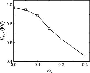
Abstract
Lateral superjunctions (LSJ) are potential candidates for CMOS compatible high voltage devices in next-generation power integrated circuits. The prior works have modeled and developed design guidelines only for an ideal balanced LSJ, i.e., having equal charge in the n- and p-pillars. However, inevitable process variation during fabrication results in charge imbalance, \({k_{N}}\), that yields a breakdown voltage, \({V_\textrm{BR}}\), significantly lower than the target breakdown voltage, \({V_\textrm{BR,target}}\). In this work, we use the method of Lagrange multipliers to derive analytical equations for the optimum pillar parameters of an LSJ; these parameters yield the minimum specific ON-resistance, \({R_\textrm{ONSP}}\), for a \({V_\textrm{BR,target}}\) and \({k_{N}}\). The analytical solutions are verified using well-calibrated TCAD simulations for 0.1–1 kV Si LSJs and 1–10 kV 4H-SiC LSJs for \({k_{N}}\) from 0.05 to 0.30 (signifying 5 to 30% imbalance between the n- and p-pillar charge). Our solutions show that the optimum aspect ratio, \({r_{0}}\), varies between 8–12 for Si LSJs and 10–15 for 4H-SiC LSJs. Notably, our solution for an LSJ is found to yield significantly different optimum pillar parameters than our earlier solution for a vertical SJ for the same \({V_\textrm{BR}}\) and \({k_{N}}\), due to the difference in their dependency of \({R_\textrm{ONSP}}\) on the pillar parameters. This justifies the need for customized solution for the design of LSJ.
横向超结(LSJ)是下一代功率集成电路中CMOS兼容高压器件的潜在候选器件。先前的工作只对理想的平衡LSJ进行了建模和开发设计指南,即在n柱和p柱中具有相等的电荷。然而,在制造过程中不可避免的工艺变化导致电荷不平衡\({k_{N}}\),从而产生击穿电压\({V_\textrm{BR}}\),显着低于目标击穿电压\({V_\textrm{BR,target}}\)。在这项工作中,我们使用拉格朗日乘子法推导了LSJ的最佳柱参数的解析方程;这些参数产生最小比导通电阻\({R_\textrm{ONSP}}\),对于\({V_\textrm{BR,target}}\)和\({k_{N}}\)。利用校准良好的TCAD模拟对0.1-1 kV Si LSJs和1-10 kV 4H-SiC LSJs进行了验证,\({k_{N}}\)范围从0.05到0.30(表示5到30)% imbalance between the n- and p-pillar charge). Our solutions show that the optimum aspect ratio, \({r_{0}}\), varies between 8–12 for Si LSJs and 10–15 for 4H-SiC LSJs. Notably, our solution for an LSJ is found to yield significantly different optimum pillar parameters than our earlier solution for a vertical SJ for the same \({V_\textrm{BR}}\) and \({k_{N}}\), due to the difference in their dependency of \({R_\textrm{ONSP}}\) on the pillar parameters. This justifies the need for customized solution for the design of LSJ.
期刊介绍:
he Journal of Computational Electronics brings together research on all aspects of modeling and simulation of modern electronics. This includes optical, electronic, mechanical, and quantum mechanical aspects, as well as research on the underlying mathematical algorithms and computational details. The related areas of energy conversion/storage and of molecular and biological systems, in which the thrust is on the charge transport, electronic, mechanical, and optical properties, are also covered.
In particular, we encourage manuscripts dealing with device simulation; with optical and optoelectronic systems and photonics; with energy storage (e.g. batteries, fuel cells) and harvesting (e.g. photovoltaic), with simulation of circuits, VLSI layout, logic and architecture (based on, for example, CMOS devices, quantum-cellular automata, QBITs, or single-electron transistors); with electromagnetic simulations (such as microwave electronics and components); or with molecular and biological systems. However, in all these cases, the submitted manuscripts should explicitly address the electronic properties of the relevant systems, materials, or devices and/or present novel contributions to the physical models, computational strategies, or numerical algorithms.

 求助内容:
求助内容: 应助结果提醒方式:


