Fe-induced stacking faults engineering for breakthrough broadband absorption in SiBCN ceramics
IF 14.3
1区 材料科学
Q1 MATERIALS SCIENCE, MULTIDISCIPLINARY
引用次数: 0
Abstract
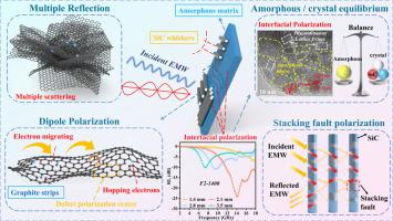
Polymer-derived SiBCN ceramics (PDCs-SiBCN) have emerged as promising candidates for high-performance electromagnetic wave absorption applications. However, their strong electromagnetic loss, attributed to high crystalline phase content, simultaneously causes impedance mismatch and a narrow absorption bandwidth. To address this challenge, this study proposes an innovative stacking faults (SFs) defect engineering strategy, which can achieve high dielectric loss at low crystallinity. Specifically, SiC whiskers with high-density SFs were catalytically grown using an Fe-mediated liquid-solid interface during polyborosilazane pyrolysis. These SFs serve as effective polarization centers, significantly enhancing dielectric loss capability. By optimizing Fe content, fewer crystalline phases and high SFs density were achieved in SiBCN, thereby realizing impedance matching and strong dielectric loss. Consequently, the unique microstructure expanded the effective absorption bandwidth of SiBCN from 4.82 to 6.36 GHz at 2.1 mm thickness, demonstrating record-breaking broadband absorption performance among PDCs. This Fe-mediated SFs defect engineering provides a strategic pathway to resolve the long-standing conflict between “impedance matching and strong dielectric loss” in PDCs.
突破SiBCN陶瓷宽带吸收的铁致层错工程
聚合物衍生的SiBCN陶瓷(PDCs-SiBCN)已成为高性能电磁波吸收应用的有前途的候选者。然而,由于高晶相含量,它们的强电磁损耗同时导致阻抗失配和窄吸收带宽。为了解决这一挑战,本研究提出了一种创新的堆叠故障(SFs)缺陷工程策略,该策略可以在低结晶度下实现高介电损耗。具体来说,在聚硼硅烷热解过程中,利用铁介导的液-固界面催化生长了具有高密度SFs的SiC晶须。这些SFs作为有效的极化中心,显著提高了介质损耗能力。通过优化铁含量,使得SiBCN的晶相减少,sf密度高,从而实现阻抗匹配和强介质损耗。因此,独特的微结构将SiBCN在2.1 mm厚度下的有效吸收带宽从4.82 GHz扩展到6.36 GHz,在PDCs中展示了破纪录的宽带吸收性能。这种fe介导的SFs缺陷工程为解决PDCs中长期存在的“阻抗匹配与强介电损耗”之间的矛盾提供了一条战略途径。
本文章由计算机程序翻译,如有差异,请以英文原文为准。
求助全文
约1分钟内获得全文
求助全文
来源期刊
Journal of Materials Science & Technology
工程技术-材料科学:综合
CiteScore
20.00
自引率
11.00%
发文量
995
审稿时长
13 days
期刊介绍:
Journal of Materials Science & Technology strives to promote global collaboration in the field of materials science and technology. It primarily publishes original research papers, invited review articles, letters, research notes, and summaries of scientific achievements. The journal covers a wide range of materials science and technology topics, including metallic materials, inorganic nonmetallic materials, and composite materials.
 求助内容:
求助内容: 应助结果提醒方式:


