S. N. Garibova, A. I. Isayev, I. A. Mamedova, M. E. Aliyev, F. Sarcan
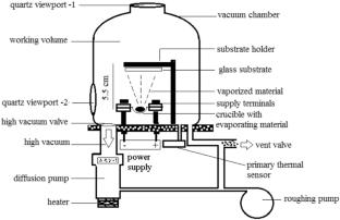
{"title":"Fabrication and structural analysis of amorphous GeTe4, Sb2Te3 and Ge20SbxTe80-x thin films prepared by thermal evaporation","authors":"S. N. Garibova, A. I. Isayev, I. A. Mamedova, M. E. Aliyev, F. Sarcan","doi":"10.1007/s10854-025-15776-x","DOIUrl":null,"url":null,"abstract":"<div><p>Amorphous Ge<sub>20</sub>Te<sub>80</sub>, Sb<sub>40</sub>Te<sub>60</sub>, and Ge<sub>20</sub>Sb<sub>x</sub>Te<sub>80-x</sub> (x = 1, 2, 5, 10) compounds were synthesized and deposited as thin films (40–80 nm) on glass substrates via thermal evaporation under high vacuum (10<sup>–5</sup> Torr). Their structural characteristics were examined using X-ray diffraction, scanning electron microscopy, and atomic-force microscopy. Applying the void–cluster model, the quasi-period of density fluctuations (r), correlation length (L), and packing fraction (L/r) were estimated from the first sharp diffraction peak in the XRD patterns. Partial substitution of Te by Sb in Ge<sub>20</sub>Te<sub>80</sub> led to a reduction in L and L/r, indicating increase in structural disorder. Raman spectroscopy revealed vibrational modes associated with short-range ordering in Ge<sub>20</sub>Te<sub>80</sub> and Sb<sub>40</sub>Te<sub>60</sub>, aiding interpretation of Ge<sub>20</sub>SbₓTe<sub>80</sub>₋ₓ films. In Ge<sub>20</sub>Te<sub>80</sub>, dominant Raman peaks at 121.5 and 139 cm<sup>−1</sup> were assigned to GeTe₄₋<sub>n</sub>Ge<sub>n</sub> (<i>n</i> = 0, 1) tetrahedra, while bands at 154–159 cm<sup>−1</sup> and 174–177 cm<sup>−1</sup> corresponded to Te chains and defective octahedral units. For Sb<sub>40</sub>Te<sub>60</sub> films, peaks at 124.5 and 142 cm<sup>−1</sup> were attributed to Sb–Te vibrations in pyramidal SbTe₃ units and distorted octahedral Sb coordination. Additional peaks at 97 and 152 cm<sup>−1</sup> were associated with Te–Te bonds, while the band at 113.5 cm<sup>−1</sup> corresponds to Sb–Te stretching modes. The Raman intensity at 121.5, 139 and 157 cm<sup>−1</sup> in Ge<sub>20</sub>Sb<sub>x</sub>Te<sub>80-x</sub> exhibits a non-monotonic dependence on Sb concentration, reaching a maximum at x = 2. A low- frequency boson peak (< 100 cm<sup>−1</sup>) observed in Sb<sub>40</sub>Te<sub>60</sub> suggests a high density of low-energy vibrational states, characteristic of disordered structure.</p></div>","PeriodicalId":646,"journal":{"name":"Journal of Materials Science: Materials in Electronics","volume":"36 27","pages":""},"PeriodicalIF":2.8000,"publicationDate":"2025-09-25","publicationTypes":"Journal Article","fieldsOfStudy":null,"isOpenAccess":false,"openAccessPdf":"","citationCount":"0","resultStr":null,"platform":"Semanticscholar","paperid":null,"PeriodicalName":"Journal of Materials Science: Materials in Electronics","FirstCategoryId":"5","ListUrlMain":"https://link.springer.com/article/10.1007/s10854-025-15776-x","RegionNum":4,"RegionCategory":"工程技术","ArticlePicture":[],"TitleCN":null,"AbstractTextCN":null,"PMCID":null,"EPubDate":"","PubModel":"","JCR":"Q2","JCRName":"ENGINEERING, ELECTRICAL & ELECTRONIC","Score":null,"Total":0}
引用次数: 0
Abstract
Amorphous Ge20Te80, Sb40Te60, and Ge20SbxTe80-x (x = 1, 2, 5, 10) compounds were synthesized and deposited as thin films (40–80 nm) on glass substrates via thermal evaporation under high vacuum (10–5 Torr). Their structural characteristics were examined using X-ray diffraction, scanning electron microscopy, and atomic-force microscopy. Applying the void–cluster model, the quasi-period of density fluctuations (r), correlation length (L), and packing fraction (L/r) were estimated from the first sharp diffraction peak in the XRD patterns. Partial substitution of Te by Sb in Ge20Te80 led to a reduction in L and L/r, indicating increase in structural disorder. Raman spectroscopy revealed vibrational modes associated with short-range ordering in Ge20Te80 and Sb40Te60, aiding interpretation of Ge20SbₓTe80₋ₓ films. In Ge20Te80, dominant Raman peaks at 121.5 and 139 cm−1 were assigned to GeTe₄₋nGen (n = 0, 1) tetrahedra, while bands at 154–159 cm−1 and 174–177 cm−1 corresponded to Te chains and defective octahedral units. For Sb40Te60 films, peaks at 124.5 and 142 cm−1 were attributed to Sb–Te vibrations in pyramidal SbTe₃ units and distorted octahedral Sb coordination. Additional peaks at 97 and 152 cm−1 were associated with Te–Te bonds, while the band at 113.5 cm−1 corresponds to Sb–Te stretching modes. The Raman intensity at 121.5, 139 and 157 cm−1 in Ge20SbxTe80-x exhibits a non-monotonic dependence on Sb concentration, reaching a maximum at x = 2. A low- frequency boson peak (< 100 cm−1) observed in Sb40Te60 suggests a high density of low-energy vibrational states, characteristic of disordered structure.
期刊介绍:
The Journal of Materials Science: Materials in Electronics is an established refereed companion to the Journal of Materials Science. It publishes papers on materials and their applications in modern electronics, covering the ground between fundamental science, such as semiconductor physics, and work concerned specifically with applications. It explores the growth and preparation of new materials, as well as their processing, fabrication, bonding and encapsulation, together with the reliability, failure analysis, quality assurance and characterization related to the whole range of applications in electronics. The Journal presents papers in newly developing fields such as low dimensional structures and devices, optoelectronics including III-V compounds, glasses and linear/non-linear crystal materials and lasers, high Tc superconductors, conducting polymers, thick film materials and new contact technologies, as well as the established electronics device and circuit materials.

 求助内容:
求助内容: 应助结果提醒方式:


