{"title":"Energy-Efficient flash ADC architecture based on MoS\\({}_2\\) transistors","authors":"Ashkan Horri","doi":"10.1007/s10470-025-02457-2","DOIUrl":null,"url":null,"abstract":"<div><p>In this paper, we utilize the advantages of Molybdenum Disulfide (MoS<span>\\({}_2\\)</span>) transistors to design a Flash analog-to-digital converter (ADC) that achieves a reduced active area and dynamic power. MoS<span>\\({}_2\\)</span> field-effect transistors (FETs) are a class of emerging devices based on two-dimensional (2D) materials, offering high ON/OFF current ratios, excellent electrostatic control, and scalability, making them suitable for next-generation low-power electronics. To eliminate static power dissipation, the proposed ADC incorporates the threshold inverter quantization (TIQ) technique. A SPICE-compatible charge-based model for MoS<span>\\({}_2\\)</span> transistor, published in the literature, is used to simulate the proposed ADC. Due to their high ON/OFF current ratio and nanoscale geometry, MoS<span>\\({}_2\\)</span> FETs enable significant reductions in ADC active area and dynamic power relative to traditional device technologies. Simulation results reveal that the differential nonlinearity (DNL) ranges of [-0.18, 0.12]LSB , and the integral nonlinearity (INL) ranges of [-0.32, 0.24]LSB, both satisfying the requirements for 4-bit resolution at a 2 V operating voltage. In addition, the low ADC active area of 3050 <span>\\(\\mu m^2\\)</span> rendering it well-suited for implementation in very large-scale integration (VLSI) circuits. Variations in process, temperature, and supply voltage affect the proposed method, and their influence on ADC performance is analyzed.</p></div>","PeriodicalId":7827,"journal":{"name":"Analog Integrated Circuits and Signal Processing","volume":"124 3","pages":""},"PeriodicalIF":1.4000,"publicationDate":"2025-07-07","publicationTypes":"Journal Article","fieldsOfStudy":null,"isOpenAccess":false,"openAccessPdf":"","citationCount":"0","resultStr":null,"platform":"Semanticscholar","paperid":null,"PeriodicalName":"Analog Integrated Circuits and Signal Processing","FirstCategoryId":"5","ListUrlMain":"https://link.springer.com/article/10.1007/s10470-025-02457-2","RegionNum":4,"RegionCategory":"工程技术","ArticlePicture":[],"TitleCN":null,"AbstractTextCN":null,"PMCID":null,"EPubDate":"","PubModel":"","JCR":"Q4","JCRName":"COMPUTER SCIENCE, HARDWARE & ARCHITECTURE","Score":null,"Total":0}
引用次数: 0
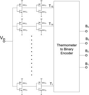
Abstract
In this paper, we utilize the advantages of Molybdenum Disulfide (MoS\({}_2\)) transistors to design a Flash analog-to-digital converter (ADC) that achieves a reduced active area and dynamic power. MoS\({}_2\) field-effect transistors (FETs) are a class of emerging devices based on two-dimensional (2D) materials, offering high ON/OFF current ratios, excellent electrostatic control, and scalability, making them suitable for next-generation low-power electronics. To eliminate static power dissipation, the proposed ADC incorporates the threshold inverter quantization (TIQ) technique. A SPICE-compatible charge-based model for MoS\({}_2\) transistor, published in the literature, is used to simulate the proposed ADC. Due to their high ON/OFF current ratio and nanoscale geometry, MoS\({}_2\) FETs enable significant reductions in ADC active area and dynamic power relative to traditional device technologies. Simulation results reveal that the differential nonlinearity (DNL) ranges of [-0.18, 0.12]LSB , and the integral nonlinearity (INL) ranges of [-0.32, 0.24]LSB, both satisfying the requirements for 4-bit resolution at a 2 V operating voltage. In addition, the low ADC active area of 3050 \(\mu m^2\) rendering it well-suited for implementation in very large-scale integration (VLSI) circuits. Variations in process, temperature, and supply voltage affect the proposed method, and their influence on ADC performance is analyzed.
期刊介绍:
Analog Integrated Circuits and Signal Processing is an archival peer reviewed journal dedicated to the design and application of analog, radio frequency (RF), and mixed signal integrated circuits (ICs) as well as signal processing circuits and systems. It features both new research results and tutorial views and reflects the large volume of cutting-edge research activity in the worldwide field today.
A partial list of topics includes analog and mixed signal interface circuits and systems; analog and RFIC design; data converters; active-RC, switched-capacitor, and continuous-time integrated filters; mixed analog/digital VLSI systems; wireless radio transceivers; clock and data recovery circuits; and high speed optoelectronic circuits and systems.

 求助内容:
求助内容: 应助结果提醒方式:


