{"title":"Study on single-event radiation effects and hardening techniques in GaN HEMTs","authors":"Yuan Liu, Ying Wang, Hao Huang","doi":"10.1007/s10825-025-02376-5","DOIUrl":null,"url":null,"abstract":"<div><p>We propose a new radiation-hardened AlGaN/GaN High Electron Mobility Transistor (N-HEMT) structure with an AlGaN insertion layer integrated into a conventional gate field-plate configuration. The AlGaN insertion layer acts as a back-barrier, effectively minimizing leakage current in the buffer layer, which in turn boosts the breakdown voltage of the device. Due to the band discontinuity and bandgap difference between AlGaN and GaN, this layer creates a quantum well at the heterojunction interface, trapping radiation-induced electrons and blocking their entry into the conductive channel. This mechanism lowers the production rate of electron–hole pairs triggered by impact ionization, significantly enhancing the device’s tolerance to single-event burnout (SEB). By optimizing parameters using Sentaurus TCAD, the reinforced structure (N-HEMT) attains a breakdown voltage of 912 V and an SEB threshold of 600 V, reflecting gains of 77 V and 350 V, respectively, compared to the conventional standard AlGaN/GaN HEMT structure (T-HEMT). While slight reductions in output and transfer performance are observed, these are considered insignificant for practical use.</p></div>","PeriodicalId":620,"journal":{"name":"Journal of Computational Electronics","volume":"24 4","pages":""},"PeriodicalIF":2.5000,"publicationDate":"2025-06-30","publicationTypes":"Journal Article","fieldsOfStudy":null,"isOpenAccess":false,"openAccessPdf":"","citationCount":"0","resultStr":null,"platform":"Semanticscholar","paperid":null,"PeriodicalName":"Journal of Computational Electronics","FirstCategoryId":"5","ListUrlMain":"https://link.springer.com/article/10.1007/s10825-025-02376-5","RegionNum":4,"RegionCategory":"工程技术","ArticlePicture":[],"TitleCN":null,"AbstractTextCN":null,"PMCID":null,"EPubDate":"","PubModel":"","JCR":"Q3","JCRName":"ENGINEERING, ELECTRICAL & ELECTRONIC","Score":null,"Total":0}
引用次数: 0
Abstract
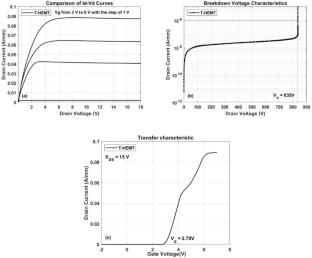
We propose a new radiation-hardened AlGaN/GaN High Electron Mobility Transistor (N-HEMT) structure with an AlGaN insertion layer integrated into a conventional gate field-plate configuration. The AlGaN insertion layer acts as a back-barrier, effectively minimizing leakage current in the buffer layer, which in turn boosts the breakdown voltage of the device. Due to the band discontinuity and bandgap difference between AlGaN and GaN, this layer creates a quantum well at the heterojunction interface, trapping radiation-induced electrons and blocking their entry into the conductive channel. This mechanism lowers the production rate of electron–hole pairs triggered by impact ionization, significantly enhancing the device’s tolerance to single-event burnout (SEB). By optimizing parameters using Sentaurus TCAD, the reinforced structure (N-HEMT) attains a breakdown voltage of 912 V and an SEB threshold of 600 V, reflecting gains of 77 V and 350 V, respectively, compared to the conventional standard AlGaN/GaN HEMT structure (T-HEMT). While slight reductions in output and transfer performance are observed, these are considered insignificant for practical use.
期刊介绍:
he Journal of Computational Electronics brings together research on all aspects of modeling and simulation of modern electronics. This includes optical, electronic, mechanical, and quantum mechanical aspects, as well as research on the underlying mathematical algorithms and computational details. The related areas of energy conversion/storage and of molecular and biological systems, in which the thrust is on the charge transport, electronic, mechanical, and optical properties, are also covered.
In particular, we encourage manuscripts dealing with device simulation; with optical and optoelectronic systems and photonics; with energy storage (e.g. batteries, fuel cells) and harvesting (e.g. photovoltaic), with simulation of circuits, VLSI layout, logic and architecture (based on, for example, CMOS devices, quantum-cellular automata, QBITs, or single-electron transistors); with electromagnetic simulations (such as microwave electronics and components); or with molecular and biological systems. However, in all these cases, the submitted manuscripts should explicitly address the electronic properties of the relevant systems, materials, or devices and/or present novel contributions to the physical models, computational strategies, or numerical algorithms.

 求助内容:
求助内容: 应助结果提醒方式:


