{"title":"Fabrication and Optical Characterization of Ultrathin Graphene Oxide Films Using a Combination Technique of Layer-by-Layer Coating Methods","authors":"M. M. Saadeldin, Ahmed Samir, A. Guirguis","doi":"10.1134/S1027451025700338","DOIUrl":null,"url":null,"abstract":"<p>The synthesis of graphene and graphene oxide (GO) is critical for unlocking their vast potential across a range of practical applications. Among the various methods employed, graphite exfoliation emerges as one of the most straightforward techniques for producing these materials. However, achieving optimal synthesis conditions, preserving the pristine structure, minimizing layers and lateral size, and reducing oxygen content present significant challenges. In this study, we focus on fabricating uniform GO thin films utilizing the intrinsic self-alignment phenomenon between scattered nanosheets, achieved through the exfoliation technique without the need for catalysis or templates. This innovative approach harnesses the natural properties of GO materials, making them more suitable for industrial applications. The electrical and optical properties of the resulting GO thin films were thoroughly characterized using microscopy, spectroscopy, and ellipsometry techniques. By classifying GO bulk material based on its electronic properties, it can be categorized as a high-energy gap semiconducting material due to the presence of both <i>sp</i><sup>3</sup> and <i>sp</i><sup>2</sup> bonds, along with abundant oxygen functional groups in its matrix. This characteristic allows for the tuning of the energy gap by controlling the oxidation/reduction level. Our findings reveal that the GO thin film with eight layers (GO<sub>8</sub>) exhibited a superior self-alignment rate compared to other films, displaying fewer defects between GO nanosheets. This GO<sub>8</sub> thin film displayed semiconducting behavior with a confined bandgap value of 2.26 eV, as determined through optical measurements. The observed self-alignment phenomenon among GO nanosheets holds promise for engineering these scattered nanosheets into more complex nanostructures, potentially enabling various applications across different fields. This study highlights the importance of understanding and harnessing inherent material properties for the development of advanced materials with tailored functionalities.</p>","PeriodicalId":671,"journal":{"name":"Journal of Surface Investigation: X-ray, Synchrotron and Neutron Techniques","volume":"19 1","pages":"224 - 237"},"PeriodicalIF":0.4000,"publicationDate":"2025-06-25","publicationTypes":"Journal Article","fieldsOfStudy":null,"isOpenAccess":false,"openAccessPdf":"","citationCount":"0","resultStr":null,"platform":"Semanticscholar","paperid":null,"PeriodicalName":"Journal of Surface Investigation: X-ray, Synchrotron and Neutron Techniques","FirstCategoryId":"1085","ListUrlMain":"https://link.springer.com/article/10.1134/S1027451025700338","RegionNum":0,"RegionCategory":null,"ArticlePicture":[],"TitleCN":null,"AbstractTextCN":null,"PMCID":null,"EPubDate":"","PubModel":"","JCR":"Q4","JCRName":"PHYSICS, CONDENSED MATTER","Score":null,"Total":0}
引用次数: 0
Abstract
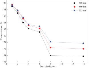
The synthesis of graphene and graphene oxide (GO) is critical for unlocking their vast potential across a range of practical applications. Among the various methods employed, graphite exfoliation emerges as one of the most straightforward techniques for producing these materials. However, achieving optimal synthesis conditions, preserving the pristine structure, minimizing layers and lateral size, and reducing oxygen content present significant challenges. In this study, we focus on fabricating uniform GO thin films utilizing the intrinsic self-alignment phenomenon between scattered nanosheets, achieved through the exfoliation technique without the need for catalysis or templates. This innovative approach harnesses the natural properties of GO materials, making them more suitable for industrial applications. The electrical and optical properties of the resulting GO thin films were thoroughly characterized using microscopy, spectroscopy, and ellipsometry techniques. By classifying GO bulk material based on its electronic properties, it can be categorized as a high-energy gap semiconducting material due to the presence of both sp3 and sp2 bonds, along with abundant oxygen functional groups in its matrix. This characteristic allows for the tuning of the energy gap by controlling the oxidation/reduction level. Our findings reveal that the GO thin film with eight layers (GO8) exhibited a superior self-alignment rate compared to other films, displaying fewer defects between GO nanosheets. This GO8 thin film displayed semiconducting behavior with a confined bandgap value of 2.26 eV, as determined through optical measurements. The observed self-alignment phenomenon among GO nanosheets holds promise for engineering these scattered nanosheets into more complex nanostructures, potentially enabling various applications across different fields. This study highlights the importance of understanding and harnessing inherent material properties for the development of advanced materials with tailored functionalities.
期刊介绍:
Journal of Surface Investigation: X-ray, Synchrotron and Neutron Techniques publishes original articles on the topical problems of solid-state physics, materials science, experimental techniques, condensed media, nanostructures, surfaces of thin films, and phase boundaries: geometric and energetical structures of surfaces, the methods of computer simulations; physical and chemical properties and their changes upon radiation and other treatments; the methods of studies of films and surface layers of crystals (XRD, XPS, synchrotron radiation, neutron and electron diffraction, electron microscopic, scanning tunneling microscopic, atomic force microscopic studies, and other methods that provide data on the surfaces and thin films). Articles related to the methods and technics of structure studies are the focus of the journal. The journal accepts manuscripts of regular articles and reviews in English or Russian language from authors of all countries. All manuscripts are peer-reviewed.
 求助内容:
求助内容: 应助结果提醒方式:


