Ibrahim L. Abdalla, Fatma A. Matter, Eslam S. El-Mokadem, Hesham F. A. Hamed, Aziza I. Hussein, Ahmed. A. Afifi
{"title":"Design and evaluation of an analytical model for one-dimensional ballistic Schottky barrier GAA carbon nanotube FETs including BTBT effects","authors":"Ibrahim L. Abdalla, Fatma A. Matter, Eslam S. El-Mokadem, Hesham F. A. Hamed, Aziza I. Hussein, Ahmed. A. Afifi","doi":"10.1007/s10825-025-02337-y","DOIUrl":null,"url":null,"abstract":"<div><p>This paper presents a novel analytical model that incorporates the band-to-band tunneling (BTBT) effect for the Schottky-barrier carbon nanotube transistor (SB-CNTFET). This advancement has paved the way for effective routes in designing and simulating ultra-scaled-down circuits. The model has been developed to provide an analytical solution to the current Landauer integral equation. To achieve this solution, approximations for the Fermi–Dirac distribution function, the band-to-band tunneling probability, and the Wentzel-Kramers-Brillouin (WKB) transmission probability have been employed. In this context, the proposed approach was utilized to model a one-dimensional (1D) Schottky barrier (SB) Gate-All-Around (GAA) CNTFET. The suggested model exhibits a high degree of agreement with experimental data, as demonstrated by the following errors: 1.6% in the threshold voltage, 4.5% in the on-current, and 1.35% in the drain-induced barrier lowering (DIBL). Furthermore, the efficiency of the proposed model is underscored by a reported computation time of approximately 1.39 s, representing a significant improvement over existing numerical models. This notable reduction in computing time highlights the advantages of employing an analytical method for CNTFET modeling. Consequently, this work successfully merges the speed and accuracy of circuit simulators.</p></div>","PeriodicalId":620,"journal":{"name":"Journal of Computational Electronics","volume":"24 4","pages":""},"PeriodicalIF":2.5000,"publicationDate":"2025-06-13","publicationTypes":"Journal Article","fieldsOfStudy":null,"isOpenAccess":false,"openAccessPdf":"","citationCount":"0","resultStr":null,"platform":"Semanticscholar","paperid":null,"PeriodicalName":"Journal of Computational Electronics","FirstCategoryId":"5","ListUrlMain":"https://link.springer.com/article/10.1007/s10825-025-02337-y","RegionNum":4,"RegionCategory":"工程技术","ArticlePicture":[],"TitleCN":null,"AbstractTextCN":null,"PMCID":null,"EPubDate":"","PubModel":"","JCR":"Q3","JCRName":"ENGINEERING, ELECTRICAL & ELECTRONIC","Score":null,"Total":0}
引用次数: 0
Abstract
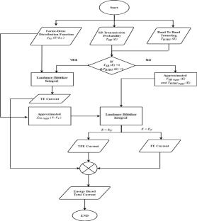
This paper presents a novel analytical model that incorporates the band-to-band tunneling (BTBT) effect for the Schottky-barrier carbon nanotube transistor (SB-CNTFET). This advancement has paved the way for effective routes in designing and simulating ultra-scaled-down circuits. The model has been developed to provide an analytical solution to the current Landauer integral equation. To achieve this solution, approximations for the Fermi–Dirac distribution function, the band-to-band tunneling probability, and the Wentzel-Kramers-Brillouin (WKB) transmission probability have been employed. In this context, the proposed approach was utilized to model a one-dimensional (1D) Schottky barrier (SB) Gate-All-Around (GAA) CNTFET. The suggested model exhibits a high degree of agreement with experimental data, as demonstrated by the following errors: 1.6% in the threshold voltage, 4.5% in the on-current, and 1.35% in the drain-induced barrier lowering (DIBL). Furthermore, the efficiency of the proposed model is underscored by a reported computation time of approximately 1.39 s, representing a significant improvement over existing numerical models. This notable reduction in computing time highlights the advantages of employing an analytical method for CNTFET modeling. Consequently, this work successfully merges the speed and accuracy of circuit simulators.
期刊介绍:
he Journal of Computational Electronics brings together research on all aspects of modeling and simulation of modern electronics. This includes optical, electronic, mechanical, and quantum mechanical aspects, as well as research on the underlying mathematical algorithms and computational details. The related areas of energy conversion/storage and of molecular and biological systems, in which the thrust is on the charge transport, electronic, mechanical, and optical properties, are also covered.
In particular, we encourage manuscripts dealing with device simulation; with optical and optoelectronic systems and photonics; with energy storage (e.g. batteries, fuel cells) and harvesting (e.g. photovoltaic), with simulation of circuits, VLSI layout, logic and architecture (based on, for example, CMOS devices, quantum-cellular automata, QBITs, or single-electron transistors); with electromagnetic simulations (such as microwave electronics and components); or with molecular and biological systems. However, in all these cases, the submitted manuscripts should explicitly address the electronic properties of the relevant systems, materials, or devices and/or present novel contributions to the physical models, computational strategies, or numerical algorithms.

 求助内容:
求助内容: 应助结果提醒方式:


