Pressure-Driven Metallicity in Ångström-Thickness 2D Bismuth and Layer-Selective Ohmic Contact to MoS2
IF 9.1
1区 材料科学
Q1 CHEMISTRY, MULTIDISCIPLINARY
引用次数: 0
Abstract
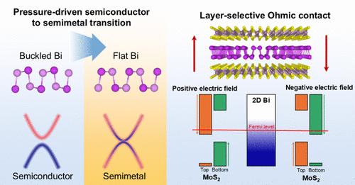
Recent fabrication of two-dimensional (2D) metallic bismuth (Bi) via van der Waals (vdW) squeezing offers a route to ultrascaling metal into ångström thickness. However, free-standing 2D Bi is typically semiconducting, which contradicts the experimentally observed metallicity in vdW-squeezed 2D Bi. Here we show that this discrepancy originates from the pressure-induced buckled-to-flat structural transition in 2D Bi, changing the electronic structures from semiconducting to semimetallic. Based on the experimentally fabricated MoS2-Bi-MoS2 trilayer heterostructure, we demonstrate the concept of layer-selective Ohmic contact in which one MoS2 layer forms an Ohmic contact to the 2D Bi while the opposite MoS2 exhibits a Schottky barrier. The Ohmic contact can be switched between the two sandwiching MoS2 monolayers by reversing an external gate field, thus enabling charge to be spatially injected into different MoS2 layers. The layer-selective Ohmic contact proposed here represents a layertronic generalization of semimetal/semiconductor contact, paving the way toward layertronic device application.
压力驱动Ångström-Thickness二维铋的金属丰度和与MoS2的层选择性欧姆接触
最近通过范德华(vdW)挤压技术制备的二维(2D)金属铋(Bi)提供了一种将金属超尺度化到ångström厚度的方法。然而,独立的二维铋是典型的半导体,这与实验观察到的vdw压缩二维铋的金属丰度相矛盾。在这里,我们表明这种差异源于压力诱导的二维Bi中的屈曲到平坦的结构转变,将电子结构从半导体变为半金属。基于实验制备的MoS2-Bi-MoS2三层异质结构,我们展示了层选择欧姆接触的概念,其中一个MoS2层与二维Bi形成欧姆接触,而另一个MoS2层则表现出肖特基势垒。通过反转外部栅极场,可以在两个夹心MoS2单层之间切换欧姆接触,从而使电荷在空间上注入到不同的MoS2层中。本文提出的层选择欧姆接触代表了半金属/半导体接触的层电子推广,为层电子器件的应用铺平了道路。
本文章由计算机程序翻译,如有差异,请以英文原文为准。
求助全文
约1分钟内获得全文
求助全文
来源期刊

Nano Letters
工程技术-材料科学:综合
CiteScore
16.80
自引率
2.80%
发文量
1182
审稿时长
1.4 months
期刊介绍:
Nano Letters serves as a dynamic platform for promptly disseminating original results in fundamental, applied, and emerging research across all facets of nanoscience and nanotechnology. A pivotal criterion for inclusion within Nano Letters is the convergence of at least two different areas or disciplines, ensuring a rich interdisciplinary scope. The journal is dedicated to fostering exploration in diverse areas, including:
- Experimental and theoretical findings on physical, chemical, and biological phenomena at the nanoscale
- Synthesis, characterization, and processing of organic, inorganic, polymer, and hybrid nanomaterials through physical, chemical, and biological methodologies
- Modeling and simulation of synthetic, assembly, and interaction processes
- Realization of integrated nanostructures and nano-engineered devices exhibiting advanced performance
- Applications of nanoscale materials in living and environmental systems
Nano Letters is committed to advancing and showcasing groundbreaking research that intersects various domains, fostering innovation and collaboration in the ever-evolving field of nanoscience and nanotechnology.
 求助内容:
求助内容: 应助结果提醒方式:


