{"title":"Identifying the Chemical Structure of Indium–Gallium–Zinc Oxide Thin Films with Oxygen Vacancy Variation","authors":"Jong-Cheol Lee, , , Jinheon Choi, , , Tackhwi Lee, , , Minsik Kim, , , Seongmin Ahn, , , Junghan Lee, , , Sungho Lee, , , Jihyun Kho, , , Yongsoon Choi, , , Kwangmin Park, , and , Cheol Seong Hwang*, ","doi":"10.1021/acsaelm.5c01023","DOIUrl":null,"url":null,"abstract":"<p >Controlling the oxygen vacancy (V<sub>O</sub>), or more precisely, the local oxygen deficiency, in amorphous oxide semiconductor InGaZnO (IGZO) thin films during device fabrication is crucial because it affects the transfer characteristics and reliability of thin-film transistor (TFT) devices. Measuring the O 1s peak in X-ray photoelectron spectroscopy (XPS) and performing peak deconvolution have been widely used to identify the V<sub>O</sub> status, where the deconvoluted O 1s peak with a binding energy (BE) between 531 and 532 eV is considered to represent V<sub>O</sub>. However, this work reveals that the In 3d<sub>5/2</sub> peak is a more reliable indicator of the V<sub>O</sub> (or carrier) concentration, where a higher In 3d<sub>5/2</sub> peak BE corresponds to a lower V<sub>O</sub> concentration and higher TFT threshold voltages. The O 1s peak at 531–532 eV BE did not originate from the oxygen ions near the V<sub>O</sub> inside the IGZO film but rather from the oxygen atoms in the acetate molecules on the surface. When the IGZO surface was contaminated by OH and CO<sub>2</sub> from the air, more acetate was formed, increasing the peak intensity. Moreover, such adsorption was more prevalent in materials exhibiting weak metal–oxygen bonds. Notably, the O 1s peak at 531–532 eV BE disappeared when the acetate on the IGZO film surface was in situ sputter-cleaned in the XPS chamber.</p>","PeriodicalId":3,"journal":{"name":"ACS Applied Electronic Materials","volume":"7 18","pages":"8393–8399"},"PeriodicalIF":4.7000,"publicationDate":"2025-09-09","publicationTypes":"Journal Article","fieldsOfStudy":null,"isOpenAccess":false,"openAccessPdf":"","citationCount":"0","resultStr":null,"platform":"Semanticscholar","paperid":null,"PeriodicalName":"ACS Applied Electronic Materials","FirstCategoryId":"88","ListUrlMain":"https://pubs.acs.org/doi/10.1021/acsaelm.5c01023","RegionNum":3,"RegionCategory":"材料科学","ArticlePicture":[],"TitleCN":null,"AbstractTextCN":null,"PMCID":null,"EPubDate":"","PubModel":"","JCR":"Q1","JCRName":"ENGINEERING, ELECTRICAL & ELECTRONIC","Score":null,"Total":0}
引用次数: 0
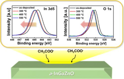
Abstract
Controlling the oxygen vacancy (VO), or more precisely, the local oxygen deficiency, in amorphous oxide semiconductor InGaZnO (IGZO) thin films during device fabrication is crucial because it affects the transfer characteristics and reliability of thin-film transistor (TFT) devices. Measuring the O 1s peak in X-ray photoelectron spectroscopy (XPS) and performing peak deconvolution have been widely used to identify the VO status, where the deconvoluted O 1s peak with a binding energy (BE) between 531 and 532 eV is considered to represent VO. However, this work reveals that the In 3d5/2 peak is a more reliable indicator of the VO (or carrier) concentration, where a higher In 3d5/2 peak BE corresponds to a lower VO concentration and higher TFT threshold voltages. The O 1s peak at 531–532 eV BE did not originate from the oxygen ions near the VO inside the IGZO film but rather from the oxygen atoms in the acetate molecules on the surface. When the IGZO surface was contaminated by OH and CO2 from the air, more acetate was formed, increasing the peak intensity. Moreover, such adsorption was more prevalent in materials exhibiting weak metal–oxygen bonds. Notably, the O 1s peak at 531–532 eV BE disappeared when the acetate on the IGZO film surface was in situ sputter-cleaned in the XPS chamber.
期刊介绍:
ACS Applied Electronic Materials is an interdisciplinary journal publishing original research covering all aspects of electronic materials. The journal is devoted to reports of new and original experimental and theoretical research of an applied nature that integrate knowledge in the areas of materials science, engineering, optics, physics, and chemistry into important applications of electronic materials. Sample research topics that span the journal's scope are inorganic, organic, ionic and polymeric materials with properties that include conducting, semiconducting, superconducting, insulating, dielectric, magnetic, optoelectronic, piezoelectric, ferroelectric and thermoelectric.
Indexed/Abstracted:
Web of Science SCIE
Scopus
CAS
INSPEC
Portico

 求助内容:
求助内容: 应助结果提醒方式:


