{"title":"Unidirectional Epitaxy of Wafer-Scale MoS2 on Sapphire via Growth Kinetics Control","authors":"Rongxiang Ding, , , Ziyang Zhang, , , Hao Wu, , , Liwei Deng, , , Yuanjian Yuan, , , Yue Huang, , , Mengjian Zhu*, , and , Ziao Tian*, ","doi":"10.1021/acsaelm.5c01522","DOIUrl":null,"url":null,"abstract":"<p >Wafer-scale single-crystalline MoS<sub>2</sub> epitaxially grown on sapphire by chemical vapor deposition (CVD) is expected to exhibit exceptional electrical and optoelectronic properties for the large-scale integration of two-dimensional (2D) semiconductor circuits. Prior studies proposed thermodynamic pathways for achieving unidirectional MoS<sub>2</sub> domains. However, thermodynamic conditions are insufficient to achieve wafer-scale growth of unidirectional MoS<sub>2</sub>, while kinetic control during epitaxy remains unexplored. Here, we demonstrate the kinetics-driven adatoms diffusion and nuclei rotation by controlling the epitaxy temperature during the CVD process. We achieve the epitaxy of triangular MoS<sub>2</sub> single-crystalline domains with a single orientation on sapphire. By carefully designing the Mo oxidation, dual-source delivery, and two-stage annealing, the nucleation density of MoS<sub>2</sub> is reduced, and the domain size and uniformity are greatly enhanced. The fine control of the growth kinetics boosts the 2 in. wafer-scale continuous MoS<sub>2</sub> single-crystalline film. The uniformity and single crystallinity were confirmed by Raman spectroscopy, photoluminescence, atomic force microscopy, low-energy electron diffraction, and second-harmonic generation. Furthermore, field-effect MoS<sub>2</sub> transistors exhibited high room-temperature mobility up to 118 cm<sup>2</sup>·V<sup>–</sup><sup>1</sup>·s<sup>–</sup><sup>1</sup>, high on/off ratio over 10<sup>10</sup>, and steep subthreshold swing of ∼85 mV·dec<sup>–1</sup>. This work not only provides a feasible strategy for the manufacture of high-quality wafer-scale MoS<sub>2</sub> films but also sheds light on the growth of other 2D semiconductor wafers.</p>","PeriodicalId":3,"journal":{"name":"ACS Applied Electronic Materials","volume":"7 18","pages":"8636–8645"},"PeriodicalIF":4.7000,"publicationDate":"2025-09-09","publicationTypes":"Journal Article","fieldsOfStudy":null,"isOpenAccess":false,"openAccessPdf":"","citationCount":"0","resultStr":null,"platform":"Semanticscholar","paperid":null,"PeriodicalName":"ACS Applied Electronic Materials","FirstCategoryId":"88","ListUrlMain":"https://pubs.acs.org/doi/10.1021/acsaelm.5c01522","RegionNum":3,"RegionCategory":"材料科学","ArticlePicture":[],"TitleCN":null,"AbstractTextCN":null,"PMCID":null,"EPubDate":"","PubModel":"","JCR":"Q1","JCRName":"ENGINEERING, ELECTRICAL & ELECTRONIC","Score":null,"Total":0}
引用次数: 0
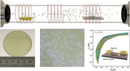
Abstract
Wafer-scale single-crystalline MoS2 epitaxially grown on sapphire by chemical vapor deposition (CVD) is expected to exhibit exceptional electrical and optoelectronic properties for the large-scale integration of two-dimensional (2D) semiconductor circuits. Prior studies proposed thermodynamic pathways for achieving unidirectional MoS2 domains. However, thermodynamic conditions are insufficient to achieve wafer-scale growth of unidirectional MoS2, while kinetic control during epitaxy remains unexplored. Here, we demonstrate the kinetics-driven adatoms diffusion and nuclei rotation by controlling the epitaxy temperature during the CVD process. We achieve the epitaxy of triangular MoS2 single-crystalline domains with a single orientation on sapphire. By carefully designing the Mo oxidation, dual-source delivery, and two-stage annealing, the nucleation density of MoS2 is reduced, and the domain size and uniformity are greatly enhanced. The fine control of the growth kinetics boosts the 2 in. wafer-scale continuous MoS2 single-crystalline film. The uniformity and single crystallinity were confirmed by Raman spectroscopy, photoluminescence, atomic force microscopy, low-energy electron diffraction, and second-harmonic generation. Furthermore, field-effect MoS2 transistors exhibited high room-temperature mobility up to 118 cm2·V–1·s–1, high on/off ratio over 1010, and steep subthreshold swing of ∼85 mV·dec–1. This work not only provides a feasible strategy for the manufacture of high-quality wafer-scale MoS2 films but also sheds light on the growth of other 2D semiconductor wafers.
期刊介绍:
ACS Applied Electronic Materials is an interdisciplinary journal publishing original research covering all aspects of electronic materials. The journal is devoted to reports of new and original experimental and theoretical research of an applied nature that integrate knowledge in the areas of materials science, engineering, optics, physics, and chemistry into important applications of electronic materials. Sample research topics that span the journal's scope are inorganic, organic, ionic and polymeric materials with properties that include conducting, semiconducting, superconducting, insulating, dielectric, magnetic, optoelectronic, piezoelectric, ferroelectric and thermoelectric.
Indexed/Abstracted:
Web of Science SCIE
Scopus
CAS
INSPEC
Portico

 求助内容:
求助内容: 应助结果提醒方式:


