{"title":"Dielectric-Engineered Monolayer MoS2 Memtransistors for Brain-Inspired Computing with High Recognition Accuracy","authors":"Manisha Rajput*, , , Sooyeon Hwang, , and , Atikur Rahman*, ","doi":"10.1021/acsami.5c11139","DOIUrl":null,"url":null,"abstract":"<p >Two-dimensional transition metal dichalcogenides (2D-TMDs)-based memtransistors have emerged as promising candidates for neuromorphic hardware due to their exceptional ability to emulate synaptic behavior. However, many existing 2D-TMDs memtransistors rely on polycrystalline channels with grain boundaries or defects introduced through postgrowth treatments, raising concerns about material integrity and the preservation of intrinsic properties. In this work, we demonstrate a monocrystalline monolayer MoS<sub>2</sub> memtransistor fabricated on a silicon nitride (SiN<sub><i>X</i></sub>) substrate, achieving a large resistive switching ratio of 10<sup>4</sup>, a dynamic range exceeding 90, along with highly linear and symmetric weight updates, minimal cycle-to-cycle variability, and low device-to-device variability. These attributes are critical for enabling high-performance neuromorphic hardware. Based on experimental data, we further show that these artificial synapses enable a recognition accuracy of more than 97% on the MNIST handwritten digits data set. Our findings present a straightforward approach to realizing 2D-TMDs memtransistors through dielectric engineering, offering a promising platform for next-generation neuromorphic computing systems.</p>","PeriodicalId":5,"journal":{"name":"ACS Applied Materials & Interfaces","volume":"17 39","pages":"55189–55198"},"PeriodicalIF":8.2000,"publicationDate":"2025-09-21","publicationTypes":"Journal Article","fieldsOfStudy":null,"isOpenAccess":false,"openAccessPdf":"","citationCount":"0","resultStr":null,"platform":"Semanticscholar","paperid":null,"PeriodicalName":"ACS Applied Materials & Interfaces","FirstCategoryId":"88","ListUrlMain":"https://pubs.acs.org/doi/10.1021/acsami.5c11139","RegionNum":2,"RegionCategory":"材料科学","ArticlePicture":[],"TitleCN":null,"AbstractTextCN":null,"PMCID":null,"EPubDate":"","PubModel":"","JCR":"Q1","JCRName":"MATERIALS SCIENCE, MULTIDISCIPLINARY","Score":null,"Total":0}
引用次数: 0
Abstract
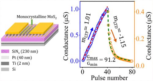
Two-dimensional transition metal dichalcogenides (2D-TMDs)-based memtransistors have emerged as promising candidates for neuromorphic hardware due to their exceptional ability to emulate synaptic behavior. However, many existing 2D-TMDs memtransistors rely on polycrystalline channels with grain boundaries or defects introduced through postgrowth treatments, raising concerns about material integrity and the preservation of intrinsic properties. In this work, we demonstrate a monocrystalline monolayer MoS2 memtransistor fabricated on a silicon nitride (SiNX) substrate, achieving a large resistive switching ratio of 104, a dynamic range exceeding 90, along with highly linear and symmetric weight updates, minimal cycle-to-cycle variability, and low device-to-device variability. These attributes are critical for enabling high-performance neuromorphic hardware. Based on experimental data, we further show that these artificial synapses enable a recognition accuracy of more than 97% on the MNIST handwritten digits data set. Our findings present a straightforward approach to realizing 2D-TMDs memtransistors through dielectric engineering, offering a promising platform for next-generation neuromorphic computing systems.
期刊介绍:
ACS Applied Materials & Interfaces is a leading interdisciplinary journal that brings together chemists, engineers, physicists, and biologists to explore the development and utilization of newly-discovered materials and interfacial processes for specific applications. Our journal has experienced remarkable growth since its establishment in 2009, both in terms of the number of articles published and the impact of the research showcased. We are proud to foster a truly global community, with the majority of published articles originating from outside the United States, reflecting the rapid growth of applied research worldwide.

 求助内容:
求助内容: 应助结果提醒方式:


