Validated multiphysics simulation of die-scale co-planarity and mass transport limitations in copper pillar electroplating
IF 5.6
3区 材料科学
Q1 ELECTROCHEMISTRY
引用次数: 0
Abstract
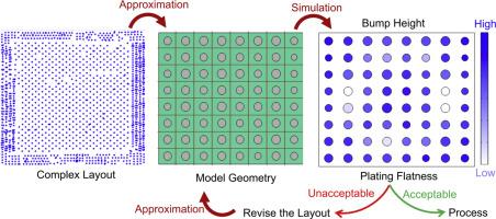
In advanced wafer-level packaging, achieving co-planarity of copper (Cu) pillars is essential for device yield and reliability, yet remains challenging due to non-uniform current distribution and localized mass transport limitations during electroplating. We present an experimentally validated, computationally efficient simulation strategy that couples multi-physics modeling of fluid dynamics, mass transport, and Butler–Volmer kinetics with a novel geometric approximation, enabling full die-scale predictions at a fraction of the computational cost of direct modeling. Complex layouts are partitioned into an N × N grid, with dense bump regions represented as equivalent circular electrodes, allowing accurate resolution of local current density and Cu2+ depletion effects. Across multiple layouts, simulated maximum and minimum bump heights deviate from experimental measurements by <1.5 %, confirming the model’s predictive capability. Analysis reveals that non-uniformity is driven by a spatially dependent transition from kinetic control to mass-transport control in densely patterned regions. Requiring only layout geometry as input, the method provides a practical tool for early-stage design screening and process optimization, reducing costly experimental iterations in advanced packaging development.

铜柱电镀模尺度共平面性和质量输运限制的多物理场仿真验证
在先进的晶圆级封装中,实现铜柱的共平面性对于器件的良率和可靠性至关重要,但由于电镀过程中电流分布不均匀和局部质量输运的限制,仍然具有挑战性。我们提出了一种实验验证的、计算效率高的模拟策略,该策略将流体动力学、质量输运和Butler-Volmer动力学的多物理场建模与一种新颖的几何近似相结合,以直接建模的一小部分计算成本实现了完整的模具规模预测。复杂的布局被划分为N × N网格,密集的凹凸区域表示为等效的圆形电极,允许精确地分辨率局部电流密度和Cu2+耗尽效应。在多种布局中,模拟的最大和最小碰撞高度与实验测量值的偏差小于1.5%,证实了模型的预测能力。分析表明,非均匀性是由密集区域的动力学控制向质量输运控制的空间依赖转变驱动的。该方法只需要布局几何作为输入,为早期设计筛选和工艺优化提供了实用工具,减少了先进封装开发中昂贵的实验迭代。
本文章由计算机程序翻译,如有差异,请以英文原文为准。
求助全文
约1分钟内获得全文
求助全文
来源期刊
Electrochimica Acta
工程技术-电化学
CiteScore
11.30
自引率
6.10%
发文量
1634
审稿时长
41 days
期刊介绍:
Electrochimica Acta is an international journal. It is intended for the publication of both original work and reviews in the field of electrochemistry. Electrochemistry should be interpreted to mean any of the research fields covered by the Divisions of the International Society of Electrochemistry listed below, as well as emerging scientific domains covered by ISE New Topics Committee.
 求助内容:
求助内容: 应助结果提醒方式:


