Viet-Anh Ha, , , Sabyasachi Tiwari, , and , Feliciano Giustino*,
{"title":"Ultrahigh Hole Mobility in Monolayer WSe2 Enabled by Spin–Orbit Suppression of Intervalley Scattering","authors":"Viet-Anh Ha, , , Sabyasachi Tiwari, , and , Feliciano Giustino*, ","doi":"10.1021/acs.nanolett.5c03258","DOIUrl":null,"url":null,"abstract":"<p >Monolayer WSe<sub>2</sub> has recently emerged as a leading candidate for ultrascaled <i>p</i>-channel transistors, with record room-temperature hole mobilities exceeding 1000 cm<sup>2</sup>/(V s). Here, we reveal the microscopic origin of this exceptional performance using state-of-the-art <i>ab initio</i> Boltzmann transport calculations, incorporating GW quasiparticle corrections and long-range dipole and quadrupole corrections for two-dimensional materials. We obtained a phonon-limited hole mobility of 931 cm<sup>2</sup>/(V s) at room temperature, in excellent agreement with experiments. We find that this exceptionally high mobility results from the combined suppression of K–K and K–K′ scattering by spin–orbit-induced valley splitting and spin-valley locking, together with intrinsically weak polar and piezoelectric interactions. These results position monolayer WSe<sub>2</sub> as a front-runner for next-generation high-mobility <i>p</i>-channel electronics and point to spin–orbit engineering as a key strategy for the design of high-mobility semiconductors.</p>","PeriodicalId":53,"journal":{"name":"Nano Letters","volume":"25 39","pages":"14304–14309"},"PeriodicalIF":9.1000,"publicationDate":"2025-09-16","publicationTypes":"Journal Article","fieldsOfStudy":null,"isOpenAccess":false,"openAccessPdf":"","citationCount":"0","resultStr":null,"platform":"Semanticscholar","paperid":null,"PeriodicalName":"Nano Letters","FirstCategoryId":"88","ListUrlMain":"https://pubs.acs.org/doi/10.1021/acs.nanolett.5c03258","RegionNum":1,"RegionCategory":"材料科学","ArticlePicture":[],"TitleCN":null,"AbstractTextCN":null,"PMCID":null,"EPubDate":"","PubModel":"","JCR":"Q1","JCRName":"CHEMISTRY, MULTIDISCIPLINARY","Score":null,"Total":0}
引用次数: 0
Abstract
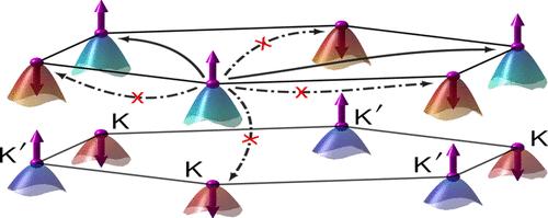
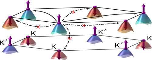
Monolayer WSe2 has recently emerged as a leading candidate for ultrascaled p-channel transistors, with record room-temperature hole mobilities exceeding 1000 cm2/(V s). Here, we reveal the microscopic origin of this exceptional performance using state-of-the-art ab initio Boltzmann transport calculations, incorporating GW quasiparticle corrections and long-range dipole and quadrupole corrections for two-dimensional materials. We obtained a phonon-limited hole mobility of 931 cm2/(V s) at room temperature, in excellent agreement with experiments. We find that this exceptionally high mobility results from the combined suppression of K–K and K–K′ scattering by spin–orbit-induced valley splitting and spin-valley locking, together with intrinsically weak polar and piezoelectric interactions. These results position monolayer WSe2 as a front-runner for next-generation high-mobility p-channel electronics and point to spin–orbit engineering as a key strategy for the design of high-mobility semiconductors.
期刊介绍:
Nano Letters serves as a dynamic platform for promptly disseminating original results in fundamental, applied, and emerging research across all facets of nanoscience and nanotechnology. A pivotal criterion for inclusion within Nano Letters is the convergence of at least two different areas or disciplines, ensuring a rich interdisciplinary scope. The journal is dedicated to fostering exploration in diverse areas, including:
- Experimental and theoretical findings on physical, chemical, and biological phenomena at the nanoscale
- Synthesis, characterization, and processing of organic, inorganic, polymer, and hybrid nanomaterials through physical, chemical, and biological methodologies
- Modeling and simulation of synthetic, assembly, and interaction processes
- Realization of integrated nanostructures and nano-engineered devices exhibiting advanced performance
- Applications of nanoscale materials in living and environmental systems
Nano Letters is committed to advancing and showcasing groundbreaking research that intersects various domains, fostering innovation and collaboration in the ever-evolving field of nanoscience and nanotechnology.

 求助内容:
求助内容: 应助结果提醒方式:


