{"title":"Patterning Halide Perovskite Monocrystalline Arrays via Dry Imprinting Transfer","authors":"Weiqi Gao, , , Kaixin Niu, , , Quanyang Tao, , , Shuimei Ding, , , Jinding Zhang, , , Linfeng Yu, , , Hongkai Zhang, , , Yuhan Liu, , , Siyu Li, , , Xiaoyu Sun, , , Yang Chen, , , Likuan Ma, , , Yaxin Zhai, , , Guangzhao Qin, , , Yiliu Wang*, , and , Yuan Liu*, ","doi":"10.1021/acsnano.5c11433","DOIUrl":null,"url":null,"abstract":"<p >Epitaxy of perovskite single crystals (SCs) has gained development, rendering large-area monocrystalline films with decent quality and high uniformity, while its patterning technologies have fallen behind due to materials degradation and contamination when processing, limiting the achievement of perovskite SC arrays and pixelization on a large scale. Here, we report a patterning method that utilizes a rigid stamper with designed geometries to mechanically punch freestanding perovskite films into SC arrays, leading to the dry patterning of perovskite SCs with high uniformity and intrinsic properties. Furthermore, arrays of complex configurations could be integrated via van der Waals (vdW) lamination, building up full-color pixel and vertical heterostructure. Based on this, we fabricated 3 × 3 photodetector arrays, with all devices exhibiting a similar responsivity of 0.5–2.6 A/W, a detectivity of 0.3–4 × 10<sup>11</sup> Jones and a fast response time of sub-20 ms. This damage- and residue-free dry imprinting transfer approach not only establishes a simple and rapid method for patterning perovskite SC arrays on a large scale, which is important for high-performance photodetectors and other optoelectronics, but also demonstrates potential for the integration of optoelectronics based on delicate semiconductors including organic thin films, 2D magnetic crystals, as well as their vdW heterostructures that are not compatible with conventional patterning techniques following the lithography-etching routine.</p>","PeriodicalId":21,"journal":{"name":"ACS Nano","volume":"19 38","pages":"34273–34282"},"PeriodicalIF":16.0000,"publicationDate":"2025-09-16","publicationTypes":"Journal Article","fieldsOfStudy":null,"isOpenAccess":false,"openAccessPdf":"","citationCount":"0","resultStr":null,"platform":"Semanticscholar","paperid":null,"PeriodicalName":"ACS Nano","FirstCategoryId":"88","ListUrlMain":"https://pubs.acs.org/doi/10.1021/acsnano.5c11433","RegionNum":1,"RegionCategory":"材料科学","ArticlePicture":[],"TitleCN":null,"AbstractTextCN":null,"PMCID":null,"EPubDate":"","PubModel":"","JCR":"Q1","JCRName":"CHEMISTRY, MULTIDISCIPLINARY","Score":null,"Total":0}
引用次数: 0
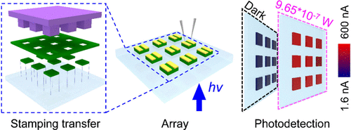
Abstract
Epitaxy of perovskite single crystals (SCs) has gained development, rendering large-area monocrystalline films with decent quality and high uniformity, while its patterning technologies have fallen behind due to materials degradation and contamination when processing, limiting the achievement of perovskite SC arrays and pixelization on a large scale. Here, we report a patterning method that utilizes a rigid stamper with designed geometries to mechanically punch freestanding perovskite films into SC arrays, leading to the dry patterning of perovskite SCs with high uniformity and intrinsic properties. Furthermore, arrays of complex configurations could be integrated via van der Waals (vdW) lamination, building up full-color pixel and vertical heterostructure. Based on this, we fabricated 3 × 3 photodetector arrays, with all devices exhibiting a similar responsivity of 0.5–2.6 A/W, a detectivity of 0.3–4 × 10¹¹ Jones and a fast response time of sub-20 ms. This damage- and residue-free dry imprinting transfer approach not only establishes a simple and rapid method for patterning perovskite SC arrays on a large scale, which is important for high-performance photodetectors and other optoelectronics, but also demonstrates potential for the integration of optoelectronics based on delicate semiconductors including organic thin films, 2D magnetic crystals, as well as their vdW heterostructures that are not compatible with conventional patterning techniques following the lithography-etching routine.
期刊介绍:
ACS Nano, published monthly, serves as an international forum for comprehensive articles on nanoscience and nanotechnology research at the intersections of chemistry, biology, materials science, physics, and engineering. The journal fosters communication among scientists in these communities, facilitating collaboration, new research opportunities, and advancements through discoveries. ACS Nano covers synthesis, assembly, characterization, theory, and simulation of nanostructures, nanobiotechnology, nanofabrication, methods and tools for nanoscience and nanotechnology, and self- and directed-assembly. Alongside original research articles, it offers thorough reviews, perspectives on cutting-edge research, and discussions envisioning the future of nanoscience and nanotechnology.


 求助内容:
求助内容: 应助结果提醒方式:


