Hydrothermally deposited Sb2S3 thin films: Effect of annealing conditions on the optoelectronic properties, the selenization, and photoelectrochemical performance
IF 6
2区 工程技术
Q2 ENERGY & FUELS
引用次数: 0
Abstract
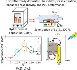
Sb2S3 is a no-toxic and earth-abundant semiconductor with suitable bandgap (1.7–1.8 eV) for opto-electronic devices operating in the UV–Vis region. It has strong optical absorption, and being a low-dimensional material shows anisotropic properties. Its favorable optoelectronic characteristics and compatibility with low-cost and scalable fabrication methods make it a strong candidate for photovoltaic and other optoelectronic applications. In this work a detailed study of the opto-electronic properties of the material Sb2S3 in relation to the post-deposition thermal processing of the thin films is discussed. The studies include the effect of annealing temperature, annealing duration, ambient pressure, and the partial substitution of sulfur (S) with selenium (Se). The studies were mainly focused on crystallite/grain orientation, Raman modes, and photocurrent response of the films subjected to the different annealing conditions. Raman analyses based on a reported empirical approach in literature showed that the quasi-1D [Sb4S6]n chains are vertical, with an inclination of ≈ 16 degrees to the normal to the substrate, which remained within a 3 % change after the different annealing processes. The temperature and pressure variation studies found that the responsivity is maximum when [Sb4S6]n chains are more closely aligned to the vertical, indicating a better charge transport. The role of S and Se vapor in the annealing chamber was manifested in the photoresponsivity. The films annealed in S atmosphere showed higher responsivity (5.29 × 10⁴ A/W) compared to those annealed without S (1.79 × 10⁴ A/W). The photoelectrochemical cell FTO/Au/Sb2(S0.71Se0.29)3/CdS achieved 6.52 mA/cm2 current at 0 vs ERHE which was further increased to 10.66 mA/cm2 at 0 vs ERHE after surface modification with Pt, attaining a PEC efficiency of 1.5 % at 0.2 ERHE.
水热沉积Sb2S3薄膜:退火条件对光电性能、硒化和光电化学性能的影响
Sb2S3是一种无毒且富含地球资源的半导体,具有合适的带隙(1.7-1.8 eV),适用于在UV-Vis区域工作的光电器件。它具有很强的光吸收性,作为一种低维材料,具有各向异性。其良好的光电特性以及与低成本和可扩展的制造方法的兼容性使其成为光伏和其他光电应用的有力候选者。在这项工作中,详细研究了材料Sb2S3的光电性质与薄膜沉积后热加工的关系。研究包括退火温度、退火时间、环境压力和硫(S)部分取代硒(Se)的影响。研究主要集中在不同退火条件下薄膜的晶体/晶粒取向、拉曼模式和光电流响应。基于文献报道的经验方法的拉曼分析表明,准一维[Sb4S6]n链是垂直的,与衬底法线的倾角约为16度,不同退火工艺后的变化幅度在3%以内。温度和压力变化研究发现,当[Sb4S6]n链与垂直方向排列更紧密时,响应性最大,表明电荷输运更好。退火室中S和Se蒸气的作用体现在光响应性上。S气氛下退火膜的响应率为5.29 × 104 A/W,高于无S气氛下退火膜的1.79 × 104 A/W。电化学电池FTO/Au/Sb2(S0.71Se0.29)3/CdS在0 vs ERHE下的电流为6.52 mA/cm2,经Pt表面改性后在0 vs ERHE下的电流进一步提高到10.66 mA/cm2,在0.2 ERHE下的PEC效率为1.5%。
本文章由计算机程序翻译,如有差异,请以英文原文为准。
求助全文
约1分钟内获得全文
求助全文
来源期刊
Solar Energy
工程技术-能源与燃料
CiteScore
13.90
自引率
9.00%
发文量
0
审稿时长
47 days
期刊介绍:
Solar Energy welcomes manuscripts presenting information not previously published in journals on any aspect of solar energy research, development, application, measurement or policy. The term "solar energy" in this context includes the indirect uses such as wind energy and biomass
 求助内容:
求助内容: 应助结果提醒方式:


