Polarization-enhanced sub-5 nm Janus MoSiGeN4 FET for high-performance and low-power applications
IF 14.3
1区 材料科学
Q1 MATERIALS SCIENCE, MULTIDISCIPLINARY
引用次数: 0
Abstract
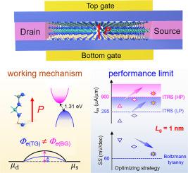
Achieving ultra-short channel field-effect transistors (FETs) that cater to both high-performance (HP) and low-power (LP) applications simultaneously is an unremitting pursuit in the field. Herein, employing first-principles calculations, we investigate the performance of sub-5 nm FETs based on the Janus MoSiGeN4 material and reveal the role of intrinsic out-of-plane electric polarization. We demonstrate that the synergistic effect of the intrinsic polarization field and the external electric field enhances the performance of Janus MoSiGeN4 FETs over MoSi2N4 and MoGe2N4 FETs. Our simulations show that a 3 nm gate-length cold-source Janus MoSiGeN4 FET, utilizing LaOCl as the dielectric material and an appropriate underlap structure, fulfills the HP and LP standards set by the International Technology Roadmap for Semiconductors (ITRS), with a subthreshold swing approaching the Boltzmann tyranny of 60 mV/dec. Notably, the optimized 1 nm gate-length MoSiGeN4 FET achieves an on-state current of 990 μΑ/μm (HP) and 690 μΑ/μm (LP), surpassing other theoretical two-dimensional FETs at the same gate length. Taking the defect effects into account, the MoSiGeN4 FET maintains a high on-state current that surpasses the ITRS for HP and LP standards. Our results provide a promising approach for designing ultra-short channel FETs suitable for both HP and LP applications.
偏振增强的亚5nm Janus MoSiGeN4场效应管,适用于高性能和低功耗应用
实现同时满足高性能(HP)和低功耗(LP)应用的超短沟道场效应晶体管(fet)是该领域的不懈追求。本文采用第一性原理计算,研究了基于Janus MoSiGeN4材料的亚5nm场效应管的性能,并揭示了本征面外电极化的作用。我们证明了本征极化场和外电场的协同效应比MoSi2N4和MoGe2N4 fet的性能更好。模拟结果表明,采用LaOCl作为介电材料和合适的下包结构的3nm栅极长Janus MoSiGeN4场效应管满足国际半导体技术路线图(ITRS)设定的HP和LP标准,亚阈值摆幅接近60 mV/dec的玻尔兹曼极限。值得注意的是,优化后的1 nm栅极长MoSiGeN4场效应管的导通电流分别为990 μΑ/μm (HP)和690 μΑ/μm (LP),超过了相同栅极长度的其他理论二维场效应管。考虑到缺陷效应,MoSiGeN4 FET保持高导通状态电流,超过HP和LP标准的ITRS。我们的研究结果为设计适用于HP和LP应用的超短通道场效应管提供了一种有前途的方法。
本文章由计算机程序翻译,如有差异,请以英文原文为准。
求助全文
约1分钟内获得全文
求助全文
来源期刊
Journal of Materials Science & Technology
工程技术-材料科学:综合
CiteScore
20.00
自引率
11.00%
发文量
995
审稿时长
13 days
期刊介绍:
Journal of Materials Science & Technology strives to promote global collaboration in the field of materials science and technology. It primarily publishes original research papers, invited review articles, letters, research notes, and summaries of scientific achievements. The journal covers a wide range of materials science and technology topics, including metallic materials, inorganic nonmetallic materials, and composite materials.
 求助内容:
求助内容: 应助结果提醒方式:


