{"title":"Color-Programmable Micro-OLED Arrays with Self-Assembled AIE Patterns","authors":"Qiuyi Zhang, Qi Huang, Zikai Zhu, Dacheng Xia, Chenxu Sheng, Shoaib Awan, Ziyang Song, Fengxian Xie, Chunxiao Cong, Zhi-Jun Qiu, Laigui Hu* and Ran Liu*, ","doi":"10.1021/acsphotonics.5c00542","DOIUrl":null,"url":null,"abstract":"<p >Although organic light-emitting diodes (OLEDs) have been widely employed in displays and flexible electronics, the implementation of micro-OLED arrays still remains a challenge due to the limitations of the mainstream fine metal mask (FMM) technology. Pixel sizes below 30 μm are typically hard to achieve in order to match the requirement (i.e., sub10 μm) of the emerging near-eye displays mainly due to the so-called “screen-door effect”. Conventional lithography used for high-resolution inorganic micro patterns cannot be directly applied owing to the instability of organic materials. Furthermore, damage-free techniques such as inkjet printing also encounter resolution limitations. Self-assembled monolayer (SAM)-assisted patterning and surface-microstructure-assisted patterning techniques, though promising, have so far only been applied to fabricate single-color micro-OLEDs. In this work, high-resolution micro-OLED arrays with dual-color emission were demonstrated using a phase-change material (PCM) or an aggregation-induced emission (AIE) material. Fabricated via the SAM-assisted patterning technique, the PCM dot array exhibits red emission in its amorphous phase and transitions to green emission upon annealing-induced crystallization. Leveraging this unique dual-color capability, micro-OLEDs with 5 μm pixels (2600 PPI) and dual-color emission were achieved after the preparation of other functional layers.</p>","PeriodicalId":23,"journal":{"name":"ACS Photonics","volume":"12 9","pages":"4932–4938"},"PeriodicalIF":6.7000,"publicationDate":"2025-08-24","publicationTypes":"Journal Article","fieldsOfStudy":null,"isOpenAccess":false,"openAccessPdf":"","citationCount":"0","resultStr":null,"platform":"Semanticscholar","paperid":null,"PeriodicalName":"ACS Photonics","FirstCategoryId":"101","ListUrlMain":"https://pubs.acs.org/doi/10.1021/acsphotonics.5c00542","RegionNum":1,"RegionCategory":"物理与天体物理","ArticlePicture":[],"TitleCN":null,"AbstractTextCN":null,"PMCID":null,"EPubDate":"","PubModel":"","JCR":"Q1","JCRName":"MATERIALS SCIENCE, MULTIDISCIPLINARY","Score":null,"Total":0}
引用次数: 0
Abstract
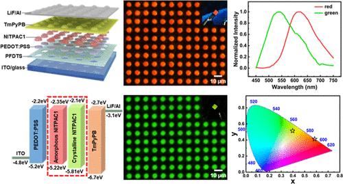
Although organic light-emitting diodes (OLEDs) have been widely employed in displays and flexible electronics, the implementation of micro-OLED arrays still remains a challenge due to the limitations of the mainstream fine metal mask (FMM) technology. Pixel sizes below 30 μm are typically hard to achieve in order to match the requirement (i.e., sub10 μm) of the emerging near-eye displays mainly due to the so-called “screen-door effect”. Conventional lithography used for high-resolution inorganic micro patterns cannot be directly applied owing to the instability of organic materials. Furthermore, damage-free techniques such as inkjet printing also encounter resolution limitations. Self-assembled monolayer (SAM)-assisted patterning and surface-microstructure-assisted patterning techniques, though promising, have so far only been applied to fabricate single-color micro-OLEDs. In this work, high-resolution micro-OLED arrays with dual-color emission were demonstrated using a phase-change material (PCM) or an aggregation-induced emission (AIE) material. Fabricated via the SAM-assisted patterning technique, the PCM dot array exhibits red emission in its amorphous phase and transitions to green emission upon annealing-induced crystallization. Leveraging this unique dual-color capability, micro-OLEDs with 5 μm pixels (2600 PPI) and dual-color emission were achieved after the preparation of other functional layers.
期刊介绍:
Published as soon as accepted and summarized in monthly issues, ACS Photonics will publish Research Articles, Letters, Perspectives, and Reviews, to encompass the full scope of published research in this field.


 求助内容:
求助内容: 应助结果提醒方式:


