{"title":"Enhanced dielectric properties and electromagnetic wave absorption in ZnO@Ni core–shell hollow spheres for Ku-band broadband applications","authors":"Omid Khanali, Khanali Nekouee, Hamed Naderi-Samani","doi":"10.1007/s10854-025-15539-8","DOIUrl":null,"url":null,"abstract":"<div><p>ZnO@Ni core–shell structures exhibit exceptional electromagnetic wave (EMW) absorption, driven by synergistic dielectric and conductive loss mechanisms. Hydrothermally synthesized ZnO hollow spheres (≈ 500 nm diameter) with hexagonal wurtzite structure were uniformly coated with a 20–60 nm Ni–P shell via electroless plating. Structural characterization (XRD, FE-SEM, TEM) confirmed the core–shell architecture, while Raman spectroscopy revealed compressive lattice stress in ZnO and enhanced defect-related polarization due to nickel deposition. The ZnO@Ni composite achieved a minimum reflection loss of − 17.4 dB at 16.5 GHz (2.3 mm thickness) and a 4.8 GHz effective bandwidth (RL < − 10 dB), significantly outperforming ZnO. This performance stems from optimized impedance matching (Z ≈ 1, 12–18 GHz), interfacial polarization at Ni–ZnO junctions, and defect-induced dipole polarization (e.g., oxygen vacancies in ZnO). Nickel’s conductivity facilitated conductive networks, boosting ohmic losses, while the hierarchical porous structure prolonged microwave propagation through multiple scattering. The core–shell design balances dielectric and conductive properties, enabling efficient energy dissipation. This work highlights ZnO@Ni’s core–shell potential as a lightweight, broadband absorber for electromagnetic shielding, leveraging interfacial engineering and defect modulation.</p></div>","PeriodicalId":646,"journal":{"name":"Journal of Materials Science: Materials in Electronics","volume":"36 24","pages":""},"PeriodicalIF":2.8000,"publicationDate":"2025-08-25","publicationTypes":"Journal Article","fieldsOfStudy":null,"isOpenAccess":false,"openAccessPdf":"","citationCount":"0","resultStr":null,"platform":"Semanticscholar","paperid":null,"PeriodicalName":"Journal of Materials Science: Materials in Electronics","FirstCategoryId":"5","ListUrlMain":"https://link.springer.com/article/10.1007/s10854-025-15539-8","RegionNum":4,"RegionCategory":"工程技术","ArticlePicture":[],"TitleCN":null,"AbstractTextCN":null,"PMCID":null,"EPubDate":"","PubModel":"","JCR":"Q2","JCRName":"ENGINEERING, ELECTRICAL & ELECTRONIC","Score":null,"Total":0}
引用次数: 0
Abstract
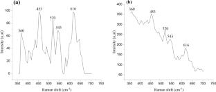
ZnO@Ni core–shell structures exhibit exceptional electromagnetic wave (EMW) absorption, driven by synergistic dielectric and conductive loss mechanisms. Hydrothermally synthesized ZnO hollow spheres (≈ 500 nm diameter) with hexagonal wurtzite structure were uniformly coated with a 20–60 nm Ni–P shell via electroless plating. Structural characterization (XRD, FE-SEM, TEM) confirmed the core–shell architecture, while Raman spectroscopy revealed compressive lattice stress in ZnO and enhanced defect-related polarization due to nickel deposition. The ZnO@Ni composite achieved a minimum reflection loss of − 17.4 dB at 16.5 GHz (2.3 mm thickness) and a 4.8 GHz effective bandwidth (RL < − 10 dB), significantly outperforming ZnO. This performance stems from optimized impedance matching (Z ≈ 1, 12–18 GHz), interfacial polarization at Ni–ZnO junctions, and defect-induced dipole polarization (e.g., oxygen vacancies in ZnO). Nickel’s conductivity facilitated conductive networks, boosting ohmic losses, while the hierarchical porous structure prolonged microwave propagation through multiple scattering. The core–shell design balances dielectric and conductive properties, enabling efficient energy dissipation. This work highlights ZnO@Ni’s core–shell potential as a lightweight, broadband absorber for electromagnetic shielding, leveraging interfacial engineering and defect modulation.
期刊介绍:
The Journal of Materials Science: Materials in Electronics is an established refereed companion to the Journal of Materials Science. It publishes papers on materials and their applications in modern electronics, covering the ground between fundamental science, such as semiconductor physics, and work concerned specifically with applications. It explores the growth and preparation of new materials, as well as their processing, fabrication, bonding and encapsulation, together with the reliability, failure analysis, quality assurance and characterization related to the whole range of applications in electronics. The Journal presents papers in newly developing fields such as low dimensional structures and devices, optoelectronics including III-V compounds, glasses and linear/non-linear crystal materials and lasers, high Tc superconductors, conducting polymers, thick film materials and new contact technologies, as well as the established electronics device and circuit materials.

 求助内容:
求助内容: 应助结果提醒方式:


