Xiaopan Song, Junyu Fan, Bin Sun, Yang Gu, Sheng Wang*, Junyang An, Duanwangde Liu, Junzhuan Wang and Linwei Yu*,
{"title":"Direct Growth and Integration of Silicon Nanowire Transistors on Polymer Substrates","authors":"Xiaopan Song, Junyu Fan, Bin Sun, Yang Gu, Sheng Wang*, Junyang An, Duanwangde Liu, Junzhuan Wang and Linwei Yu*, ","doi":"10.1021/acsami.5c11278","DOIUrl":null,"url":null,"abstract":"<p >The direct low-temperature synthesis of crystalline silicon nanowires (c-SiNWs) on flexible polymer substrates remains a critical yet unrealized milestone for scalable flexible thin-film transistors (TFTs), hindered by the interfacial mechanical mismatch between rigid silicon and deformable polymers and the ultralow thermal budgets imposed by the flexible substrates. Though nanoscale SiNW channels can be patterned/grown and transferred onto polymer substrates, high-precision postgrowth transferring and alignment of these tiny SiNW channels remain technically difficult or too cost-intensive for the implementation of large-area electronics. Here, we demonstrate a direct growth of orderly c-SiNW channels upon a flexible polyimide (PI) film for the first time, through an in-plane solid–liquid–solid (IPSLS) mechanism at 200 °C, achieving uniform diameters of 44 ± 5 nm. The prototype flexible SiNW TFT can endure a bending radius of 6.5 mm for 10,000 cycles, while achieving a high <i>I</i><sub>on</sub>/<i>I</i><sub>off</sub> current ratio of ∼5 × 10<sup>5</sup>, working stably in an ambient environment over 10 months without any passivation protection. These results represent the first experimental evidence that c-Si electronics can also be grown and integrated upon low-cost flexible substrate, opening a straightforward routine to harness the mature and stable c-Si device performance for future flexible electronics, optoelectronics.</p>","PeriodicalId":5,"journal":{"name":"ACS Applied Materials & Interfaces","volume":"17 34","pages":"48503–48510"},"PeriodicalIF":8.2000,"publicationDate":"2025-08-18","publicationTypes":"Journal Article","fieldsOfStudy":null,"isOpenAccess":false,"openAccessPdf":"","citationCount":"0","resultStr":null,"platform":"Semanticscholar","paperid":null,"PeriodicalName":"ACS Applied Materials & Interfaces","FirstCategoryId":"88","ListUrlMain":"https://pubs.acs.org/doi/10.1021/acsami.5c11278","RegionNum":2,"RegionCategory":"材料科学","ArticlePicture":[],"TitleCN":null,"AbstractTextCN":null,"PMCID":null,"EPubDate":"","PubModel":"","JCR":"Q1","JCRName":"MATERIALS SCIENCE, MULTIDISCIPLINARY","Score":null,"Total":0}
引用次数: 0
Abstract
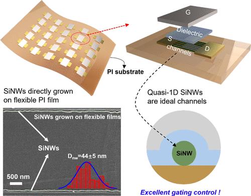
The direct low-temperature synthesis of crystalline silicon nanowires (c-SiNWs) on flexible polymer substrates remains a critical yet unrealized milestone for scalable flexible thin-film transistors (TFTs), hindered by the interfacial mechanical mismatch between rigid silicon and deformable polymers and the ultralow thermal budgets imposed by the flexible substrates. Though nanoscale SiNW channels can be patterned/grown and transferred onto polymer substrates, high-precision postgrowth transferring and alignment of these tiny SiNW channels remain technically difficult or too cost-intensive for the implementation of large-area electronics. Here, we demonstrate a direct growth of orderly c-SiNW channels upon a flexible polyimide (PI) film for the first time, through an in-plane solid–liquid–solid (IPSLS) mechanism at 200 °C, achieving uniform diameters of 44 ± 5 nm. The prototype flexible SiNW TFT can endure a bending radius of 6.5 mm for 10,000 cycles, while achieving a high Ion/Ioff current ratio of ∼5 × 10⁵, working stably in an ambient environment over 10 months without any passivation protection. These results represent the first experimental evidence that c-Si electronics can also be grown and integrated upon low-cost flexible substrate, opening a straightforward routine to harness the mature and stable c-Si device performance for future flexible electronics, optoelectronics.
期刊介绍:
ACS Applied Materials & Interfaces is a leading interdisciplinary journal that brings together chemists, engineers, physicists, and biologists to explore the development and utilization of newly-discovered materials and interfacial processes for specific applications. Our journal has experienced remarkable growth since its establishment in 2009, both in terms of the number of articles published and the impact of the research showcased. We are proud to foster a truly global community, with the majority of published articles originating from outside the United States, reflecting the rapid growth of applied research worldwide.

 求助内容:
求助内容: 应助结果提醒方式:


