Low embodied energy and carbon, high lifetime silicon boules via a combined chemical vapor deposition/float zone process
IF 6.3
2区 材料科学
Q2 ENERGY & FUELS
引用次数: 0
Abstract
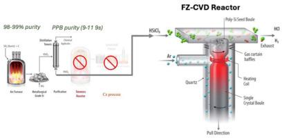
This work evaluates a new process route to making float zone (Fz)-quality silicon wafers using a combination of computational fluid dynamics (CFD) modeling and technoeconomic analysis. Our analysis finds that the new process competes with Czochralski (Cz)-grown wafers on a levelized cost of energy system level. The new process also decreases embodied energy and carbon of silicon photovoltaics (PV) by ∼6x circumventing the energy-costly Siemens process used in polycrystalline silicon (poly-Si) production plants to generate feedstock for Fz and Cz boules. Instead of using poly-Si from the Siemens process to feed crystallization, the new process uses the high-purity, trichlorosilane (TCS) precursor gas to grow a poly-Si feed rod in-situ during a modified Fz1,2 boule growth process. The gas-to-boule float zone process enables opportunity to produce high-purity (low metals and oxygen content), uniformly doped single crystal silicon boules and wafers with high bulk lifetimes (τbulk > 15 ms) to enable higher efficiency cells (>27 %) with fewer known degradation mechanisms than Czochralski (Cz)-grown wafers. These benefits reduce the levelized cost of electricity (LCOE) of PV-produced electricity. Here we show the results of our CFD and chemical modeling of the process to prove feasibility and economic viability.
低能耗和低碳,高寿命硅球通过化学气相沉积/浮子区工艺组合
本文采用计算流体动力学(CFD)建模和技术经济分析相结合的方法,评估了一种制造浮区(Fz)质量硅片的新工艺路线。我们的分析发现,新工艺在能源系统水平上与Cz生长晶圆竞争。新工艺还减少了硅光伏(PV)的蕴含能量和碳,绕过了多晶硅(poly-Si)生产工厂中使用的能源昂贵的西门子工艺,以产生Fz和Cz孔的原料。新工艺采用高纯度的三氯硅烷(TCS)前驱体气体,在改进的fz1,2孔生长过程中原位生长多晶硅进料棒,而不是使用西门子工艺的多晶硅进料棒。气-球浮区工艺使生产高纯度(低金属和低氧含量)、均匀掺杂的单晶硅球和具有高体寿命(τbulk >;15毫秒),使电池效率更高(> 27%),已知的降解机制比Cz生长的晶圆更少。这些好处降低了光伏发电的平均电力成本(LCOE)。在这里,我们展示了我们的CFD和化学模型的结果,以证明该过程的可行性和经济可行性。
本文章由计算机程序翻译,如有差异,请以英文原文为准。
求助全文
约1分钟内获得全文
求助全文
来源期刊
Solar Energy Materials and Solar Cells
工程技术-材料科学:综合
CiteScore
12.60
自引率
11.60%
发文量
513
审稿时长
47 days
期刊介绍:
Solar Energy Materials & Solar Cells is intended as a vehicle for the dissemination of research results on materials science and technology related to photovoltaic, photothermal and photoelectrochemical solar energy conversion. Materials science is taken in the broadest possible sense and encompasses physics, chemistry, optics, materials fabrication and analysis for all types of materials.
 求助内容:
求助内容: 应助结果提醒方式:


