Reliable fabrication of nanoscale Cr patterns with dry lift-off process for hard mask applications in microelectronics
IF 3.1
4区 工程技术
Q2 ENGINEERING, ELECTRICAL & ELECTRONIC
引用次数: 0
Abstract
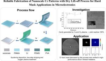
The fabrication of high-resolution and high-dense Cr masks is critical for precise pattern transfer in reactive etching processes. Lift-off based on electron-beam lithography is a commonly used and simple method for fabricating Cr nanostructures below 100-nm scale. However, conventional wet lift-off method suffers from issues such as fragment residues and low yield. In this work, we propose a dry lift-off method leveraging the weak adhesion between sputtered materials and PMMA resist to achieve high-yield (∼100 %) fabrication of high-resolution (line width<100 nm) and high-dense (gap<100 nm) Cr nanostructures that wet lift-off can hardly achieve. We demonstrate the application capability of our method by fabricating silicon infrared metalens using Cr nanostructures as etching hard masks, showing its potential for nanodevices fabrication with high-resolution and high-dense requirements.
在微电子硬掩模应用中,用干式剥离工艺可靠地制造纳米级Cr图案
在反应蚀刻工艺中,高分辨率和高密度Cr掩模的制作对于精确的图案转移至关重要。电子束刻蚀技术是制备100纳米以下铬纳米结构的一种常用且简单的方法。然而,传统的湿提法存在碎片残留和收率低等问题。在这项工作中,我们提出了一种干式剥离方法,利用溅射材料和PMMA抗蚀剂之间的弱粘附性,实现高成品率(~ 100%)制造高分辨率(线宽<; 100nm)和高密度(间隙<; 100nm)的Cr纳米结构,而湿式剥离很难实现。我们通过使用Cr纳米结构作为蚀刻硬掩膜制备硅红外超构透镜,证明了该方法的应用能力,显示了其在高分辨率和高密度要求的纳米器件制造中的潜力。
本文章由计算机程序翻译,如有差异,请以英文原文为准。
求助全文
约1分钟内获得全文
求助全文
来源期刊

Microelectronic Engineering
工程技术-工程:电子与电气
CiteScore
5.30
自引率
4.30%
发文量
131
审稿时长
29 days
期刊介绍:
Microelectronic Engineering is the premier nanoprocessing, and nanotechnology journal focusing on fabrication of electronic, photonic, bioelectronic, electromechanic and fluidic devices and systems, and their applications in the broad areas of electronics, photonics, energy, life sciences, and environment. It covers also the expanding interdisciplinary field of "more than Moore" and "beyond Moore" integrated nanoelectronics / photonics and micro-/nano-/bio-systems. Through its unique mixture of peer-reviewed articles, reviews, accelerated publications, short and Technical notes, and the latest research news on key developments, Microelectronic Engineering provides comprehensive coverage of this exciting, interdisciplinary and dynamic new field for researchers in academia and professionals in industry.
 求助内容:
求助内容: 应助结果提醒方式:


