Pablo Casado, Michele Pisarra, Fabian Calleja, Cristina Díaz, Fernando Martín, Amadeo L. Vázquez de Parga and Manuela Garnica
{"title":"Defect identification in monolayer MoTe2 through tunneling tip-induced charging and theoretical analysis","authors":"Pablo Casado, Michele Pisarra, Fabian Calleja, Cristina Díaz, Fernando Martín, Amadeo L. Vázquez de Parga and Manuela Garnica","doi":"10.1039/D5NA00501A","DOIUrl":null,"url":null,"abstract":"<p >Defects in transition metal dichalcogenides (TMDs) are pivotal in modulating their electronic, optical, and catalytic properties. Investigating these defects is essential for advancing both fundamental knowledge and practical applications. In this study, we examine the individual defects in a monolayer of MoTe<small><sub>2</sub></small> supported on graphene grown on an Ir(111) substrate by means of scanning tunneling microscopy (STM). Charging rings appear at distinct bias voltages, revealing ionization levels of doping centers located either below or above the Fermi level. Although direct STM visualization of point defects was not achieved, the combination of scanning tunneling spectroscopy (STS) and density functional theory (DFT) calculations enabled the identification of the structural origins of the charge states. Our results demonstrate a powerful tool for uncovering the electronic and structural characteristics of atomic-scale defects in MoTe<small><sub>2</sub></small>, contributing to the understanding of defect-driven electronic properties in transition metal dichalcogenides.</p>","PeriodicalId":18806,"journal":{"name":"Nanoscale Advances","volume":" 18","pages":" 5637-5645"},"PeriodicalIF":4.6000,"publicationDate":"2025-08-08","publicationTypes":"Journal Article","fieldsOfStudy":null,"isOpenAccess":false,"openAccessPdf":"https://www.ncbi.nlm.nih.gov/pmc/articles/PMC12334125/pdf/","citationCount":"0","resultStr":null,"platform":"Semanticscholar","paperid":null,"PeriodicalName":"Nanoscale Advances","FirstCategoryId":"88","ListUrlMain":"https://pubs.rsc.org/en/content/articlelanding/2025/na/d5na00501a","RegionNum":3,"RegionCategory":"材料科学","ArticlePicture":[],"TitleCN":null,"AbstractTextCN":null,"PMCID":null,"EPubDate":"","PubModel":"","JCR":"Q2","JCRName":"CHEMISTRY, MULTIDISCIPLINARY","Score":null,"Total":0}
引用次数: 0
Abstract
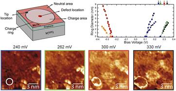
Defects in transition metal dichalcogenides (TMDs) are pivotal in modulating their electronic, optical, and catalytic properties. Investigating these defects is essential for advancing both fundamental knowledge and practical applications. In this study, we examine the individual defects in a monolayer of MoTe2 supported on graphene grown on an Ir(111) substrate by means of scanning tunneling microscopy (STM). Charging rings appear at distinct bias voltages, revealing ionization levels of doping centers located either below or above the Fermi level. Although direct STM visualization of point defects was not achieved, the combination of scanning tunneling spectroscopy (STS) and density functional theory (DFT) calculations enabled the identification of the structural origins of the charge states. Our results demonstrate a powerful tool for uncovering the electronic and structural characteristics of atomic-scale defects in MoTe2, contributing to the understanding of defect-driven electronic properties in transition metal dichalcogenides.
 求助内容:
求助内容: 应助结果提醒方式:


